ZHCSFS6B July 2016 – June 2018 SN65DSI85-Q1
PRODUCTION DATA.
- 1 特性
- 2 应用
- 3 说明
- 4 修订历史记录
- 5 Pin Configuration and Functions
- 6 Specifications
- 7 Parameter Measurement Information
-
8 Detailed Description
- 8.1 Overview
- 8.2 Functional Block Diagram
- 8.3 Feature Description
- 8.4 Device Functional Modes
- 8.5 Programming
- 8.6
Register Maps
- 8.6.1 Local I2C Interface Overview
- 8.6.2 Control and Status Registers Overview
- 8.6.3
CSR Bit
- 8.6.3.1 ID Registers (address = 0x00 to 0x08)
- 8.6.3.2 Reset and Clock Registers
- 8.6.3.3 DSI Registers
- 8.6.3.4 LVDS Registers
- 8.6.3.5
Video Registers
- 8.6.3.5.1 Address 0x20
- 8.6.3.5.2 Address 0x21
- 8.6.3.5.3 Address 0x22
- 8.6.3.5.4 Address 0x23
- 8.6.3.5.5 Address 0x24
- 8.6.3.5.6 Address 0x25
- 8.6.3.5.7 Address 0x26
- 8.6.3.5.8 Address 0x27
- 8.6.3.5.9 Address 0x28
- 8.6.3.5.10 Address 0x29
- 8.6.3.5.11 Address 0x2A
- 8.6.3.5.12 Address 0x2B
- 8.6.3.5.13 Address 0x2C
- 8.6.3.5.14 Address 0x2D
- 8.6.3.5.15 Address 0x2E
- 8.6.3.5.16 Address 0x2F
- 8.6.3.5.17 Address 0x30
- 8.6.3.5.18 Address 0x31
- 8.6.3.5.19 Address 0x32
- 8.6.3.5.20 Address 0x33
- 8.6.3.5.21 Address 0x34
- 8.6.3.5.22 Address 0x35
- 8.6.3.5.23 Address 0x36
- 8.6.3.5.24 Address 0x37
- 8.6.3.5.25 Address 0x38
- 8.6.3.5.26 Address 0x39
- 8.6.3.5.27 Address 0x3A
- 8.6.3.5.28 Address 0x3B
- 8.6.3.5.29 Address 0x3C
- 8.6.3.5.30 Address 0x3D
- 8.6.3.5.31 Address 0x3E
- 8.6.3.6 IRQ Registers
- 9 Application and Implementation
- 10Power Supply Recommendations
- 11Layout
- 12器件和文档支持
- 13机械、封装和可订购信息
8.3.1 Reset Implementation
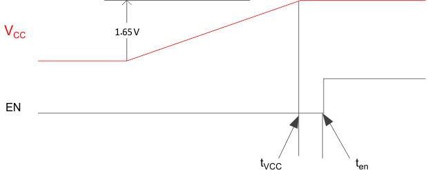
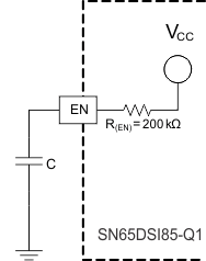
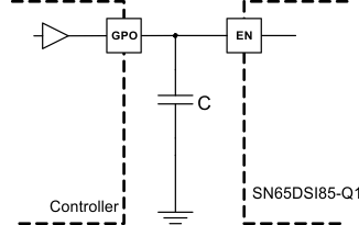
When the EN pin is deasserted (low), the SN65DSI85-Q1 device is in SHUTDOWN or RESET state. In this state, CMOS inputs are ignored, the MIPI D-PHY inputs are disabled and outputs are high impedance. Transitioning the EN input from a low to a high level after the VCC supply has reached the minimum operating voltage as shown in Figure 6 is critical. This transition is achieved by a control signal to the EN input, or by an external capacitor connected between EN and GND.
 Figure 6. Cold-Start VCC Ramp Up to EN
 When implementing the external capacitor, the size of the external capacitor depends on the power up ramp of the VCC supply, where a slower ramp-up results in a larger value external capacitor. See the latest reference schematic for the SN65DSI85-Q1 device and, or consider an approximately 200-nF capacitor as a reasonable first estimate for the size of the external capacitor.
Figure 7 and Figure 8 show both EN implementations.
 Figure 7. External Capacitor Controlled EN
  Figure 8. EN Input from Active Controller
 When the SN65DSI85-Q1 is reset while VCC is high, the EN pin must be held low for at least 10 ms before being asserted high as described in Table 1 to be sure that the device is properly reset. The DSI CLK lane MUST be in HS and the DSI data lanes MUST be driven to LP11 while the device is in reset before the EN pin is asserted per the timing described in Table 1.