ZHCSDD1A July 2014 – December 2015 SN65DSI86-Q1
PRODUCTION DATA.
- 1 特性
- 2 应用
- 3 说明
- 4 修订历史记录
- 5 说明 (续)
- 6 Pin Configuration and Functions
- 7 Specifications
-
8 Detailed Description
- 8.1 Overview
- 8.2 Functional Block Diagram
- 8.3 Feature Description
- 8.4
Device Functional Modes
- 8.4.1 Reset Implementation
- 8.4.2 Power-Up Sequence
- 8.4.3 Power Down Sequence
- 8.4.4 Display Serial Interface (DSI)
- 8.4.5
DisplayPort
- 8.4.5.1 HPD (Hot Plug/Unplug Detection)
- 8.4.5.2 AUX_CH
- 8.4.5.3 I2C-Over-AUX
- 8.4.5.4 DisplayPort PLL
- 8.4.5.5 DP Output VOD and Pre-emphasis Settings
- 8.4.5.6 DP Main Link Configurability
- 8.4.5.7 DP Main Link Training
- 8.4.5.8 Panel Size vs DP Configuration
- 8.4.5.9 Panel Self Refresh (PSR)
- 8.4.5.10 Secondary Data Packet (SDP)
- 8.4.5.11 Color Bar Generator
- 8.4.5.12 DP Pattern
- 8.4.5.13 BPP Conversion
- 8.5 Programming
- 8.6 Register Map
- 9 Application and Implementation
- 10Power Supply Recommendations
- 11Layout
- 12器件和文档支持
- 13机械、封装和可订购信息
7 Specifications
7.1 Absolute Maximum Ratings
over operating free-air temperature range (unless otherwise noted)(1)| MIN | MAX | UNIT | ||
|---|---|---|---|---|
| Supply voltage | VCCA, VCC | –0.3 | 1.3 | V |
| VCCIO, VPLL | –0.3 | 2.175 | ||
| Input voltage | All input terminals | –0.5 | 2.175 | V |
| Operating temperature | –40 | 85 | °C | |
| Storage temperature, Tstg | –65 | 105 | °C | |
(1) Stresses beyond those listed under Absolute Maximum Ratings may cause permanent damage to the device. These are stress ratings only, which do not imply functional operation of the device at these or any other conditions beyond those indicated under Recommended Operating Conditions. Exposure to absolute-maximum-rated conditions for extended periods may affect device reliability.
7.2 Handling Ratings
| MIN | MAX | UNIT | ||||
|---|---|---|---|---|---|---|
| Tstg | Storage temperature range | –65 | 150 | °C | ||
| V(ESD) | Electrostatic discharge | Human body model (HBM), per AEC Q100-002 Classification Level H2, all pins(1) | –2000 | 2000 | V | |
| Charged device model (CDM), per AEC Q100-011 Classification Level C4B | Corner pins | –750 | 750 | |||
| Other pins | –500 | 500 | ||||
(1) AEC Q100-002 indicates HBM stressing is done in accordance with the ANSI/ESDA/JEDEC JS-001 specification.
7.3 Recommended Operating Conditions
over operating free-air temperature range (unless otherwise noted)| MIN | NOM | MAX | UNIT | ||
|---|---|---|---|---|---|
| VCCA | VCCA Power supply; analog circuits | 1.14 | 1.2 | 1.26 | V |
| VCC | VCC Power supply; digital circuits | 1.14 | 1.2 | 1.26 | V |
| VCCIO | VCCIO Power Supply; digital IOs. | 1.65 | 1.8 | 1.98 | V |
| VPLL | VPLL Power Supply, DisplayPort PLL | 1.65 | 1.8 | 1.98 | V |
| VPSN | Supply noise on any VCC terminal | f(noise) > 1 MHz | 0.05 | V | |
| VDSI_PIN | DSI input pin voltage range | –50 | 1350 | mV | |
| f(I2C) | Local I2C input frequency | 400 | kHz | ||
| fHS_CLK | DSI HS clock input frequency | 40 | 750 | MHz | |
| ZL | DP output differential load impedance | 90 | 110 | Ω | |
| TA | Operating free-air temperature | –40 | 85 | °C | |
| TJ | Operating junction temperature | –40 | 105 | °C | |
7.4 Thermal Information
| THERMAL METRIC(1) | SN65DSI86-Q1 | UNIT | |
|---|---|---|---|
| PAP | |||
| 64 TERMINALS | |||
| RθJA | Junction-to-ambient thermal resistance | 35.5 | °C/W |
| RθJC(top) | Junction-to-case (top) thermal resistance | 17.7 | °C/W |
| RθJB | Junction-to-board thermal resistance | 19.5 | °C/W |
| ψJT | Junction-to-top thermal resistance metric (High-K board(1)) | 0.7 | °C/W |
| ψJB | Junction-to-board thermal resistance metric (High-K board(1)) | 19.4 | °C/W |
| RθJC(bot) | Junction-to-case (bottom) thermal resistance | 1.7 | °C/W |
(1) For more information about traditional and new thermal metrics, see the Semiconductor and IC Package Thermal Metrics application report, SPRA953.
7.5 Electrical Characteristics
over operating free-air temperature range (unless otherwise noted)| PARAMETER | TEST CONDITIONS | MIN | TYP(1) | MAX | UNIT | |
|---|---|---|---|---|---|---|
| STANDARD IO (TEST1, TEST2, ADDR, SCL, SDA, IRQ, REFCLK, EN, GPIO[4:1]) | ||||||
| VIL | Low-level control signal input voltage | 0.3 × VCCIO |
V | |||
| VIH | High-level control signal input voltage | 0.7 × VCCIO |
V | |||
| VOH | High-level output voltage | IOH = –2 mA | 1.3 | V | ||
| VOL | Low-level output voltage | IOL = 2 mA | 0.4 | V | ||
| IIH | High-level input current | Any input terminal | ±5 | μA | ||
| IIL | Low-level input current | |||||
| IOZ | High-impedance output current | Any output terminal | ±10 | μA | ||
| IOS | Short-circuit output current | Any output driving GND short | ±2 | mA | ||
| ICCA | VCCA device active current | VCCA = 1.2 V (2) | 70 | 126 | mA | |
| ICC | VCC device active current | VCCA = 1.2 V (2) | 43 | 52 | mA | |
| ICCIO | VCCIO and VPLL device active current | VCCIO = 1.8 V, VPLL = 1.8 V (2) | 32 | 32 | mA | |
| ISUSPEND_CCA | VCCA device suspend current | All data and clock lanes are in ultra-low power state (ULPS) and SUSPEND = 1 | 9.8 | mA | ||
| ISUSPEND_CC | VCC device suspend current | All data and clock lanes are in ultra-low power state (ULPS) and SUSPEND = 1 | 9 | mA | ||
| ISUSPEND_CCIO | VCCIO and VPLL device suspend current | All data and clock lanes are in ultra-low power state (ULPS) and SUSPEND = 1 | 1.16 | mA | ||
| IEN_CCA | VCCA shutdown current | EN = 0 | 0.95 | mA | ||
| IEN_CC | VCC shutdown current | EN = 0 | 2 | mA | ||
| IEN_CCIO | VCCIO and VPLL shutdown current | EN = 0 | 0.038 | mA | ||
| REN | EN control input resistor | 150 | kΩ | |||
| ADDR, EN, SCL, SDA, DBP/N[3:0], DAP/N[3:1], DBCP/N, DACP/N | ||||||
| ILEAK | Input failsafe leakage current | VCC = 0; VCCIO = 0 V. Input pulled up to VCCIO max. DSI inputs pulled up to 1.3 V | –40 | 40 | µA | |
| MIPI DSI INTERFACE | ||||||
| VIH-LP | LP receiver input high threshold | See Figure 5 | 880 | mV | ||
| VIL-LP | LP receiver input low threshold | 550 | mV | |||
| VOH-LP | LP transmitter high-level output voltage | 1100 | 1300 | mV | ||
| VOL-LP | LP transmitter low-level output voltage | –50 | 50 | mV | ||
| VIHCD | LP Logic 1 contention threshold | 450 | mV | |||
| VILCD | LP Logic 0 contention threshold | 200 | mV | |||
| |VID| | HS differential input voltage | 70 | 270 | mV | ||
| |VIDT| | HS differential input voltage threshold | 50 | mV | |||
| VIL-ULPS | LP receiver input low threshold; ultra-low power state (ULPS) | 300 | mV | |||
| VCM-HS | HS common mode voltage; steady-state | 70 | 330 | mV | ||
| ΔVCM-HS | HS common mode peak-to-peak variation including symbol delta and interference | 100 | mV | |||
| VIH-HS | HS single-ended input high voltage | See Figure 5 | 460 | mV | ||
| VIL-HS | HS single-ended input low voltage | –40 | mV | |||
| VTERM-EN | HS termination enable; single-ended input voltage (both Dp AND Dn apply to enable) | Termination is switched simultaneous for Dn and Dp | 450 | mV | ||
| RDIFF-HS | HS mode differential input impedance | 80 | 125 | Ω | ||
| DisplayPort MAIN LINK | ||||||
| VTX_DC_CM | Output common mode voltage | 0 | 2 | V | ||
| VTX_AC_CM_HBR_RBR | TX AC common mode voltage for HBR and RBR. | 20 | mVRMS | |||
| VTX_AC_CM_HBR2 | TX AC common mode voltage for HBR2 | 30 | mVRMS | |||
| VTX_DIFFPP_LVL0 | Differential peak-to-peak output voltage level 0 | Based on default state of V0_P0_VOD register | 300 | 400 | 460 | mV |
| VTX_DIFFPP_LVL1 | Differential peak-to-peak output voltage level 1 | Based on default state of V1_P0_VOD register | 450 | 600 | 690 | mV |
| VTX_DIFFPP_LVL2 | Differential peak-to-peak output voltage level 2 | Based on default state of V2_P0_VOD register | 600 | 800 | 920 | mV |
| VTX_DIFFPP_LVL3 | Differential peak-to-peak output voltage level 3 | Based on default state of V3_P0_VOD register. Level 3 is not enabled by default | 600 | 800 | 920 | mV |
| VTX_PRE_RATIO_0 | Pre-emphasis level 0 | 0 | 0 | 0 | dB | |
| VTX_PRE_RATIO_1 | Pre-emphasis level 1 | 2.8 | 3.5 | 4.2 | dB | |
| VTX_PRE_RATIO_2 | Pre-emphasis level 2 | 4.8 | 6.0 | 7.2 | dB | |
| VTX_PRE_RATIO_3 | Pre-emphasis level 3 | Level 3 is not enabled by default | 4.8 | 6.0 | 7.2 | dB |
| VTX_PRE_POST2_RATIO_0 | Post-cursor2 level 0 | 0 | 0 | 0 | dB | |
| VTX_PRE_POST2_RATIO_1 | Post-cursor2 level 1 | –1.1 | –0.9 | –0.7 | dB | |
| VTX_PRE_POST2_RATIO_2 | Post-cursor2 level 2 | –2.3 | –1.9 | –1.5 | dB | |
| VTX_PRE_POST2_RATIO_3 | Post-cursor2 level 3 | Level 3 is not enabled by default | –3.7 | –3.1 | –2.5 | dB |
| ITX_SHORT | TX short circuit current limit | 50 | mA | |||
| RTX_DIFF | Differential impedance | 80 | 100 | 120 | Ω | |
| CAC_COUPLING | AC coupling capacitor | 75 | 200 | nF | ||
| DisplayPort HPD | ||||||
| VHPD_PLUG | Hot plug detection threshold | Measured at 51-kΩ series resistor. | 2.2 | V | ||
| VHPD_UNPLUG | Hot unplug detection threshold | Measured at 51-kΩ series resistor. | 0.8 | V | ||
| RHPDPD | HPD internal pulldown resistor | 51 | 60 | 69 | kΩ | |
| DisplayPort AUX INTERFACE | ||||||
| VAUX_DIFF_PP_TX | Peak-to-peak differential voltage at transmit pins | VAUX_DIFF_PP = 2 × |VAUXP – VAUXN| | 0.18 | 1.38 | V | |
| VAUX_DIFF_PP_RX | Peak-to-peak differential voltage at receive pins | VAUX_DIFF_PP = 2 × |VAUXP – VAUXN| | 0.18 | 1.36 | V | |
| RAUX_TERM | AUX channel termination DC resistance | 100 | Ω | |||
| VAUX_DC_CM | AUX channel DC common mode voltage | 0 | 1.2 | V | ||
| VAUX_TURN_CM | AUX channel turnaround common-mode voltage | 0.3 | V | |||
| IAUX_SHORT | AUX Channel short circuit current limit | 90 | mA | |||
| CAUX | AUX AC-coupling capacitor | 75 | 200 | nF | ||
(1) All typical values are at VCC = 1.2 V, VCCA = 1.2 V, VCCIO = 1.8 V, and VPLL = 1.8 V, and TA = 25°C
(2) Maximum condition: WQXGA 60 fps Dual-Link 2xDP at HBR2, PLL enabled; typical condition: WUXGA 60 fps 1xDP at HBR2, PLL enabled
7.6 Timing Requirements
| MIN | MAX | UNIT | ||
|---|---|---|---|---|
| Power-up For DPPLL_CLK_SRC = REFCLK, See Figure 1 | ||||
| td1 | VCC/A stable before VCCIO/VPLL stable | 0 | µs | |
| td2 | VCC/A and VCCIO/VPLL stable before EN assertion | 100 | µs | |
| td3 | REFCLK active and stable before EN assertion | 0 | µs | |
| td4 | GPIO[3:1] stable before EN assertion | 0 | ns | |
| td5 | GPIO[3:1] stable after EN assertion | 5 | µs | |
| td6 | LP11 state on DSI channels A and B before EN assertion | 0 | ns | |
| td7 | LP11 state on DSI channels A and B after EN assertion(1) | 100 | µs | |
| tVCC_RAMP | VCC supply ramp requirements | 0.2 | 100 | ms |
| tVCCA_RAMP | VCCA supply ramp requirements | 0.2 | 100 | ms |
| tVCCIO_RAMP | VCCIO supply ramp requirements | 0.2 | 100 | ms |
| tVPLL_RAMP | VPLL supply ramp requirements | 0.2 | 100 | ms |
| Power-up For DPPLL_CLK_SRC = DACP/N, See Figure 2 | ||||
| td1 | VCC/A stable before VCCIO/VPLLstable | 0 | µs | |
| td2 | VCC/A and VCCIO/VPLL stable before EN assertion | 100 | µs | |
| td3 | REFCLK low before EN assertion | 10 | µs | |
| td4 | GPIO[3:1] stable before EN assertion | 0 | ns | |
| td5 | GPIO[3:1] stable after EN assertion | 5 | µs | |
| td6 | LP11 state on DSI channels A and B before EN assertion | 0 | ns | |
| td7 | LP11 state on DSI channels A and B after EN assertion(1) | 100 | µs | |
| td8 | DACP/N active and stable before DP_PLL_EN bit is set. | 100 | µs | |
| tVCC_RAMP | VCC supply ramp requirements | 0.2 | 100 | ms |
| tVCCA_RAMP | VCCA supply ramp requirements | 0.2 | 100 | ms |
| tVCCIO_RAMP | VCCIO supply ramp requirements | 0.2 | 100 | ms |
| tVPLL_RAMP | VPLL supply ramp requirements | 0.2 | 100 | ms |
| SUSPEND Timing Requirements, See Figure 3 | ||||
| td1 | LP11 or ULPS on DSI channel A and B before assertion of SUSPEND. | 200 | ns | |
| td2 | Delay from SUSPEND asserted to DisplayPort Main Link powered off. | 2 × tREFCLK | ||
| td3 | REFCLK active hold time after assertion of SUSPEND | 4 × tREFCLK | ||
| td4 | REFCLK active setup time before deassertion of SUSPEND. | 100 | ns | |
| td5 | Delay from SUSPEND deasserted to DisplayPort Main Link active and transmitting IDLE pattern. Semi-Auto Link Training is NOT used. | 20 + (1155 × tREFCLK) | µs | |
| td6 | LP11 state or ULPS on DSI channels A and B after SUSPEND deassertion | 20 + (1155 × tREFCLK) | µs | |
(1) Access to DSIx6 CFR from I2C or DSI allowed after td7.
7.7 Switching Characteristics
over operating free-air temperature range (unless otherwise noted)| PARAMETER | TEST CONDITIONS | MIN | TYP(1) | MAX | UNIT | |
|---|---|---|---|---|---|---|
| MIPI DSI INTERFACE | ||||||
| tGS | DSI LP glitch suppression pulse width | 300 | ps | |||
| tHS-SETUP | DSI HS data to clock setup time | 0.2 | UI | |||
| tHS-HOLD | DSI HS clock to data hold time | 0.2 | UI | |||
| DisplayPort MAIN LINK | ||||||
| FBR7 | Bit rate 7 | 5.37138 | 5.4 | 5.40162 | Gbps | |
| FBR6 | Bit rate 6 | 4.297104 | 4.32 | 4.321296 | Gbps | |
| FBR5 | Bit rate 5 | 3.222828 | 3.24 | 3.240972 | Gbps | |
| FBR4 | Bit rate 4 | 2.68569 | 2.7 | 2.70081 | Gbps | |
| FBR3 | Bit rate 3 | 2.417121 | 2.43 | 2.430729 | Gbps | |
| FBR2 | Bit rate 2 | 2.148552 | 2.16 | 2.160648 | Gbps | |
| FBR1 | Bit rate 1 | 1.611414 | 1.62 | 1.620486 | Gbps | |
| UIBR7 | Unit interval for BR7 | High limit = +300 ppm. Low limit = –5300 ppm |
185 | ps | ||
| UIBR6 | Unit interval for BR6 | High limit = +300 ppm. Low limit = –5300 ppm |
231.5 | ps | ||
| UIBR5 | Unit interval for BR5 | High limit = +300 ppm. Low limit = –5300 ppm |
308.6 | ps | ||
| UIBR4 | Unit interval for BR4 | High limit = +300 ppm. Low limit = –5300 ppm |
370.4 | ps | ||
| UIBR3 | Unit interval for BR3 | High limit = +300 ppm. Low limit = –5300 ppm |
411.5 | ps | ||
| UIBR2 | Unit interval for BR2 | High limit = +300 ppm. Low limit = –5300 ppm |
463 | ps | ||
| UIBR1 | Unit interval for BR1 | High limit = +300 ppm. Low limit = –5300 ppm |
617.3 | ps | ||
| tERC_L0 | Differential output rise or fall time with DP_ERC set to 0 | 50 | 61 | 80 | ps | |
| tERC_L1 | Differential output rise or fall time with DP_ERC set to 1 | 74 | 95 | 115 | ps | |
| tERC_L2 | Differential output rise or fall time with DP_ERC set to 2 | 108 | 123 | 146 | ps | |
| tERC_L3 | Differential output rise or fall time with DP_ERC set to 3 | 136 | 153 | 168 | ps | |
| tTX_RISE_FALL
_MISMATCH |
Lane intra-pair output skew at TX pins | 5% | ||||
| tINTRA_SKEW | Intra-pair differential skew | 20 | ps | |||
| tINTER_SKEW | Inter-pair differential skew | 100 | ps | |||
| tTX_EYE_HBR2 | Minimum TX eye width at TX package pins for HBR2(2) | 0.73 | UIHBR2 | |||
| tTX_EYE_MED_TO
_MAX_JIT_HBR2 |
Maximum time between the jitter median and maximum deviation from the median at TX package pins for HBR2(2) | 0.135 | UIHBR2 | |||
| tTX_EYE_HBR | Minimum TX eye width at TX package pins for HBR(2) | 0.72 | UIHBR | |||
| tTX_EYE_MED_TO
_MAX_JIT_HBR |
Maximum time between the jitter median and maximum deviation from the median at TX package pins for HBR(2) | 0.147 | UIHBR | |||
| tTX_EYE_RBR | Minimum TX eye width at TX package pins for RBR(2) | 0.82 | UIRBR | |||
| tTX_EYE_MED_TO
_MAX_JIT_RBR |
Maximum time between the jitter median and maximum deviation from the median at TX package pins for RBR(2) | 0.09 | UIRBR | |||
| tXSSC_AMP | Link clock down-spreading | 0% | 0.5% | |||
| tSSC_FREQ | Link clock down-spreading frequency | 30 | 33 | kHz | ||
| DisplayPort AUX INTERFACE | ||||||
| UIMAN | Manchester transaction unit interval | 0.4 | 0.6 | µs | ||
| tauxjitter_tx | Cycle-to-cycle jitter time at transmit pins | 0.08 | UIMAN | |||
| tauxjitter_rx | Cycle-to-cycle jitter time at receive pins | 0.04 | UIMAN | |||
| REFCLK | ||||||
| fREFCLK | REFCLK frequency. supported frequencies: 12 MHz, 19.2 MHz, 26 MHz, 27 MHz, 38.4 MHz | 12 | 38.4 | MHz | ||
| tRISEFALL | REFCLK rise or fall time | 10% to 90% | 100 ps | 23 | ns | |
| tREFCLK | REFCLK period | 26.0417 | 83.333 | ns | ||
| tpj | REFCLK peak-to-peak phase jitter | 50 | ps | |||
| Duty | REFCLK duty cycle | 40% | 50% | 60% | ||
(1) All typical values are at VCC = 1.2 V and TA = 25 °C
(2) BR refers to BR1; HBR refers to BR; HBR2 refers to BR7.
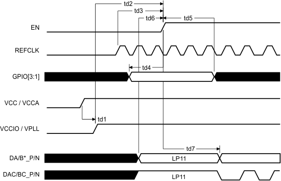 Figure 1. Power-Up Timing Definitions for DPPLL_CLK_SRC = REFCLK
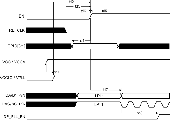 Figure 2. Power-Up Timing Definitions for DPPLL_CLK_SRC = DACP/N
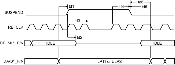 Figure 3. SUSPEND Timing Definitions
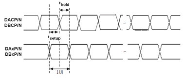 Figure 4. DSI HS Mode Receiver Timing Definitions
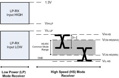 Figure 5. DSI Receiver Voltage Definitions