ZHCSBP5C september 2013 – october 2020 SN65DSI86
PRODUCTION DATA
- 1
- 1 特性
- 2 应用
- 3 说明
- 4 Revision History
- 5 Description (continued)
- 6 Pin Configuration and Functions
- 7 Specifications
-
8 Detailed Description
- 8.1 Overview
- 8.2 Functional Block Diagram
- 8.3 Feature Description
- 8.4
Device Functional Modes
- 8.4.1 Reset Implementation
- 8.4.2 Power-Up Sequence
- 8.4.3 Power Down Sequence
- 8.4.4 Display Serial Interface (DSI)
- 8.4.5
DisplayPort
- 8.4.5.1 HPD (Hot Plug/Unplug Detection)
- 8.4.5.2 AUX_CH
- 8.4.5.3 I2C-Over-AUX
- 8.4.5.4 DisplayPort PLL
- 8.4.5.5 DP Output VOD and Pre-emphasis Settings
- 8.4.5.6 DP Main Link Configurability
- 8.4.5.7 DP Main Link Training
- 8.4.5.8 Panel Size vs DP Configuration
- 8.4.5.9 Panel Self Refresh (PSR)
- 8.4.5.10 Secondary Data Packet (SDP)
- 8.4.5.11 Color Bar Generator
- 8.4.5.12 DP Pattern
- 8.4.5.13 BPP Conversion
- 8.5 Programming
- 8.6 Register Map
- 9 Application and Implementation
- 10Power Supply Recommendations
- 11Layout
- 12Device and Documentation Support
- 13Mechanical, Packaging, and Orderable Information
8.4.4.5 DSI Video Transmission Specifications
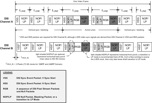
The SN65DSI86 expects the GPU to provide video timing events and active pixel data in the proper order in the form of a real-time pixel stream. According to the DSI specification [DSI], active pixel data is transmitted in one of two modes: Non-Burst and Burst. The SN65DSI86 supports both non-burst and burst mode packet transmission. The burst mode supports time-compressed pixel stream packets that leave added time per scan line for power savings LP mode. For a robust and low-power implementation, the transition to LP mode is recommended on every video line, although once per frame is considered acceptable.
According to the DSI specification [DSI], timing events can be provided in one of two types: Sync Pulses, and Sync Events. The vsupports both types. For the Sync Pulse type of timing event, the GPU will send VSYNC START (VSS), VSYNC END (VSE), HSYNC START (HSS), and HSYNC END (HSE) packets. For Sync Event type, the GPU will only send the sync start packets (VSS and HSS). For both types of timing events, the DSIx6 will use the values programmed into the Video Registers to determine the sync end events (VSE and HSE). Please note when configured for dual DSI channels, the SN65DSI86 will use VSS, VSE, and HSS packets from channel A. The DSIx6 will use channel A events to recreate the same timings on the DisplayPort interface. The VSS, VSE, and HSS packets from channel B are used to internally align data on channel B to channel A.
The first line of a video frame must start with a VSS packet, and all other lines start with VSE or HSS. The position of the synchronization packets in time is of utmost importance because this has a direct impact on the visual performance of the display panel.
As required in the DSI specification, the v requires that pixel stream packets contain an integer number of pixels (that is, end on a pixel boundary); TI recommends to transmit an entire scan line on one pixel stream packet. When a scan line is broken in to multiple packets, inter-packet latency must be considered such that the video pipeline (that is, pixel queue or partial line buffer) does not run empty (that is, under-run); during scan line processing. If the pixel queue runs empty, the SN65DSI86 transmits zero data (18’b0 or 24’b0) on the DisplayPort interface.
When configured for dual DSI channels, the SN65DSI86 supports ODD/EVEN configurations and LEFT/RIGHT configurations. In the ODD/EVEN configuration, the odd pixels for each scan line are received on channel A, and the even pixels are received on channel B. In LEFT/RIGHT mode, the left portion of the line is received on channel A, and the right portion of the line is received on channel B. The pixels received on channel B in LEFT/RIGHT mode are buffered during the left-side transmission to DisplayPort, and begin transmission to DisplayPort when the left-side input buffer runs empty. The only requirement for LEFT/RIGHT mode is CHB_ACTIVE_LINE_LENGTH must be at least 1 pixel.
The DSIx6 does not support the DSI Virtual Channel capability.
| NUMBER | REQUIREMENT |
|---|---|
| 1 | DSI datatypes VSS and HSS are required, but datatypes HSE and VSE are optional. |
| 2 | The exact time interval between each HSS must be maintained. |
| 3 | The time between the HSS and HACT (known as HBP) does not have to be maintained. The DSIx6 will recreate HBP on DisplayPort. |
| 4 | The time from the end of HACT to HSS (known as HFP) does not have to be maintained. The DSIx6 will recreate HFP on DisplayPort. |
| 5 | The time from VSS to first line of active video must be maintained. |
| 6 | The time from end of last line of active video to the beginning of the first line of active video must be maintained. This time is defined as the Vertical Blanking period. |
 Figure 8-10 DSI Channel Transmission and Transfer Function