ZHCSRU7E november 2002 – march 2023 SN65HVD08 , SN75HVD08
PRODUCTION DATA
- 1 特性
- 2 应用
- 3 说明
- 4 Revision History
- 5 Pin Configuration and Functions
- 6 Specifications
- 7 Parameter Measurement Information
- 8 Detailed Description
- 9 Application and Implementation
- 10Device and Documentation Support
- 11Mechanical, Packaging, and Orderable Information
9.1.2 Opto-Isolated Data Buses
Long RS-485 circuits can create large ground loops and pick up common-mode noise voltages in excess of the range tolerated by standard RS-485 circuits. A common remedy is to provide galvanic isolation of the data circuit from earth or local grounds.
Transformers, capacitors, or phototransistors most often provide isolation of the bus and the local node. Transformers and capacitors require changing signals to transfer the information over the isolation barrier and phototransistors (opto-isolators) can pass steady-state signals. Each of these methods incurs additional costs and complexity, the former in clock encoding and decoding of the data stream and the latter in requiring an isolated power supply.
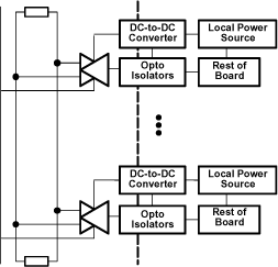
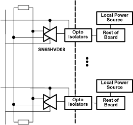
Quite often, the cost of isolated power is repeated at each node connected to the bus as shown in Figure 9-2. The possibly lower-cost solution is to generate this supply once within the system and then distribute it along with the data line(s) as shown in Figure 9-3.
 Figure 9-2 Isolated Power at Each Node
 Figure 9-3 Distribution of Isolated Power
The features of the SN65HVD08 are particularly good for the application of Figure 9-3. Due to added supply source impedance, the low quiescent current requirements and wide supply voltage tolerance allow for the poorer load regulation.