ZHCS233D May 2011 – May 2017 SN65HVD101 , SN65HVD102
PRODUCTION DATA.
- 1 特性
- 2 应用
- 3 说明
- 4 修订历史记录
- 5 Device Comparison Table
- 6 Pin Configuration and Functions
- 7 Specifications
- 8 Parameter Measurement
-
9 Detailed Description
- 9.1 Overview
- 9.2 Functional Block Diagram
- 9.3
Feature Description
- 9.3.1 Wake-up Detection
- 9.3.2 Current Limit Indication - Short Circuit Current Detection
- 9.3.3 Active Current Limit Condition: VTHL > VCQ ≥ VTHH
- 9.3.4 Inactive Current Limit Condition: VTHL < VCQ < VTHH
- 9.3.5 Over-temperature Detection
- 9.3.6 CQ Current-limit Adjustment
- 9.3.7 Transceiver Function Tables
- 9.3.8 Voltage Regulator (Not Available in SN65HVD102)
- 9.4 Device Functional Modes
- 10Application and Implementation
- 11Power Supply Recommendations
- 12Layout
- 13器件和文档支持
- 14机械、封装和可订购信息
10 Application and Implementation
NOTE
Information in the following applications sections is not part of the TI component specification, and TI does not warrant its accuracy or completeness. TI’s customers are responsible for determining suitability of components for their purposes. Customers should validate and test their design implementation to confirm system functionality.
10.1 Application Information
The SN65HVD101 and SN65HVD102 IO-Link transceivers can be used in slave devices communicating with an IO-Link master, or as simple digital I/O to either sense or drive a wide range of sensors and loads.
10.2 Typical Application
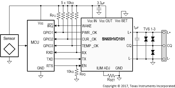 Figure 11. Typical Application Schematic, SN65HVD101 with 3.3V Output Supply
10.2.1 Design Requirements
For this design example, use the parameters listed in Table 10 as design parameters.
Table 10. Design Parameters
| DESIGN PARAMETER | EXAMPLE VALUE | |
|---|---|---|
| TRANSCEIVER | Input voltage range (L+) | 24V |
| Maximum load current (CQ) | 250 mA | |
| Output voltage (Vcc_OUT) | 3.3 V | |
| Maximum output current (Vcc_OUT) | 20 mA | |
| SURGE PROTECTION | Peak Voltage (L+, CQ) | 2 kV |
| (1.2/50 – 8/20μs) | Peak Current via R = 500 Ω, C = 0.5 µF | 4 A |
| Maximum TVS Clamping Voltage | > 50 V | |
| Minimum TVS Standoff Voltage | > 30 V | |
| Maximum Ambient Temperature, TA | 100 °C | |
| Maximum Junction Temperature, TJ | 150 °C | |
10.2.2 Detailed Design Procedure
The following recommendations on device configuration and components selection focus on the design of a digital output driver using SN65HVD101 with protection against surge transients from a 1.2/50 – 8/20 μs combination waveform generator (CWG) with 2 kV peak test voltage and 500 Ω source impedance.
10.2.2.1 Transceiver Configuration (SN65HVD101)
- Choose a 24 V nominal dc supply for L+.
- From the current-limit characteristics in Figure 2 derive the resistor value of RSET = 4 kΩ for a current limit of IO(LIM) = 250 mA.
- Connect VCC_SET to ground for a 3.3V output at VCC_OUT.
- Connect VCC_IN to VCC_OUT to assure proper output voltage regulation of VCC_OUT.
- Buffer VCC_OUT with a 3.3μF, 10V ceramic capacitor.
- Connect the receiver and diagnostic outputs via 10 kΩ pull-up resistors to VCC_OUT to provide defined voltage potentials to the controller inputs during high-impedance states.
- Connect the driver enable pin, EN, via a 10 kΩ pull-down resistor to ground to maintain the driver disabled during power up.
10.2.2.2 Maximum Ambient Temperature Check
For a 250 mA current limit, the maximum voltage drop across the high-side switch is given with VRQH = 3 V (taken from Electrical Characteristics: Driver section). This causes an internal power consumption of:

Multiply this value with the Junction-to-ambient thermal resistance of θJA = 33.8 °C/W (taken from Thermal Information) to receive the difference between junction temperature, TJ, and ambient temperature, TA:

Add this value to the maximum ambient temperature of TA = 100 °C to receive the final junction temperature:

As long as TJ-max is below the recommended maximum value of 150 °C, no overheating will occur.
10.2.2.3 Transient Protection
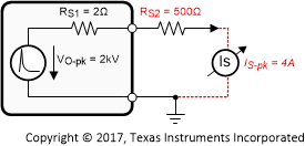
A commonly applied surge immunity test in digital I/O designs is the application of the 1.2/50 – 8/20 μs combination waveform, specified in IEC61000-4-5, with a source impedance of 500 Ω and a peak test voltage of VO-pk = 2 kV, which results in a peak surge current of IS-pk = 4 A.
The test set-up for line-to-line and line-to-ground measurements is shown in Figure 12; the calculation of the surge peak current is shown in Figure 13.
 Figure 12. Surge Test Set-up Figure 12. Surge Test Set-up
|
|
|
10.2.2.4 TVS Evaluation
Because the maximum transceiver supply at L+ is specified with 30 V, the TVS standoff or peak working voltage must be higher than this value. The standoff voltage is the voltage where the TVS does not conduct yet. Transient voltage suppressors with this high standoff have peak pulse powers starting at 200 W. Their peak pulse power however is usually rated based on a 10/1000 μs current pulse, which is commonly applied in telecom application. It is therefore necessary to derate the peak power value from a 10/1000 μs to a 8/20 μs pulse.
For this example the bidirectional, 200 W TVS, SMF33CA, was selected. Its main parameters and their derated values are listed in Table 11. The peak pulse power rating for a 10/1000 μs pulse is shown in Figure 14.
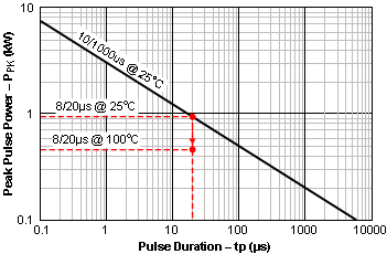 Figure 14. Peak Pulse Power Rating
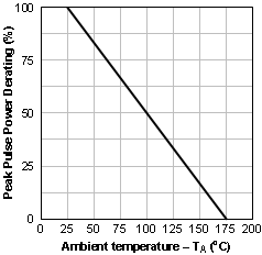 Figure 15. Pulse Derating Curve
At the pulse duration of 1000 μs the device has a peak pulse power rating of 200 W. To determine the peak power for a 8/20 μs pulse, move up the power rating curve until you hit the 20 μs pulse duration. The peak pulse power rating at this point is about 950 W.
Note these values are valid for 25 °C ambient temperature only. Because the operating ambient temperature in this example is specified with 100 °C however, the peak pulse power must be further derated for the higher ambient temperature using the pulse derating curve in Figure 15. This curve shows that the peak power level at 25 °C drops by 50 % when reaching 100 °C, so from 950 W down to 475 W. This drop is shown in Figure 14 through the arrow pointing down to the second peak power level for a 20 μs pulse duration at 100 °C.
Table 11. TVS Parameters
| PARAMETER | SYMBOL | SMF33CA | UNIT |
|---|---|---|---|
| Maximum Working Peak Voltage | VWM | 33 | V |
| Minimum Breakdown Voltage at 1 mA | VBR | 36.7 | V |
| Maximum Clamping Voltage at IPP | VCL | 53.3 | V |
| Peak Pulse Power (10/1000 μs) at 25°C | PPK1 | 200 | W |
| Peak Pulse Current (10/1000 μs) at 25°C | IPP1 | 3.75 | A |
| Derated Peak Power (8/20 μs) at 25°C | PPK2 | 950 | W |
| Derated Peak Current (8/20 μs) at 25°C | IPP2 | 17.76 | A |
| Derated Peak Power (8/20 μs) at 100°C | PPK3 | 475 | W |
| Derated Peak Current (8/20 μs) at 100°C | IPP3 | 8.9 | A |
To determine the peak currents for the various peak power ratings, TVS manufacturers advise to assume the maximum clamping voltage as being constant, because this clamping level also presents the device maximum failing voltage if its value is exceeded. The peak current for a given power rating is therefore calculated via:

So for the 8/20 μs peak power of 475 W at 100 °C, the peak pulse current is IPP3 = 475 W ÷ 53.3 V = 8.9 A. The new derived values of PPK and IPP in combination with the values for breakdown and clamping voltage, VBR and VCL, from Table 11, yield a new I-V characteristics of the SMF33CA TVS when exposed to a 8/20 μs pulse.
 Figure 16. TVS Characteristic for 8/20 μs Current Pulse
Because the maximum surge current of the CWG in Figure 13 is only 4 A at 2 kV test voltage, the TVS clamping voltage at this level is only 44 V. This voltage is sufficiently below the absolute maximum voltage rating of 50 V for a 100 μs pulse at the L+ and CQ terminals of the SN65HVD101 and SN65HVD102 transceivers, causing no device damage.
10.2.3 Application Curves
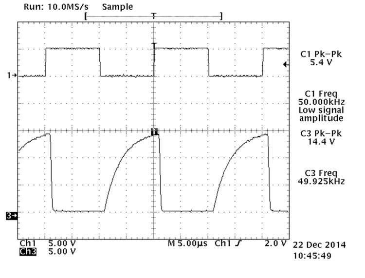
| N-Switch Mode | TX pin High | |
| Top waveform = EN | Bottom waveform = CQ | |
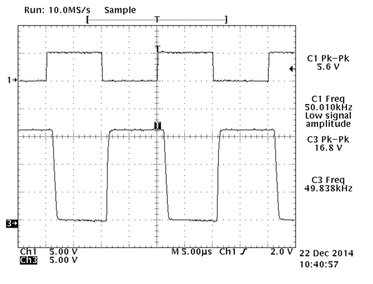
| Push-Pull Mode | EN pin High | |
| Top waveform = TX | Bottom waveform = CQ | |

| VCC (top) and ICC (bottom) at Start-Up without 3.3 µF LDO Output Capacitor | ||

| P-Switch Mode | TX pin Low | |
| Top waveform = EN | Bottom waveform = CQ | |

| VCC (top) and ICC (bottom) at Start-Up with 3.3 µF LDO Output Capacitor | ||
10.3 System Examples
10.3.1 Driver for Incandescent Lamp Loads
The following circuit shows the SN65HVD101 driving an incandescent lamp load. For this and other types of resistive loads only two TVS diodes are used to protect the CQ and L+ lines to ground.
 Figure 17. SN65HVD101 Driving Incandescent Lamp Load
The resistance of an incandescent lamp filament varies strongly with temperature. The initial (cold-filament) resistance of tungsten-filament lamps is less than 10% of the steady-state (hot-filament) resistance. For example, a 100-watt, 120-volt lamp has a resistance of 144 Ω when lit, but the cold resistance is much lower (about 9.5 Ω). The initial “in-rush” current is therefore high compared to the steady-state current. Within 3 to 5 ms the current falls to approximately half the hot current.
For typical general-service lamps, the current reaches steady-state conditions in less than about 100 milliseconds. The ‘HVD10x CQ output will remain at the selected current-limit as the filament warms up, and then will stay at the steady-state current level. For example, a 6W, 24VDC indicator lamp has a steady-state current of 250 mA. However, the initial in-rush current could be over 2 Amps if unlimited. If the HVD10x current limit is set to 350 mA, this current will warm up the filament during the initial lamp turn-on, and the final current will be below the current limit. If the CQ output current is at the limit for longer than tSC, the SC output will be active. The local controller can disable the CQ driver if the high current is not expected, or can re-check the SC output after 100 ms if the load is known to be incandescent.
10.3.2 Driver for Inductive Loads
The following circuit shows the SN65HVD101 driving an inductive load. In this case three TVS diodes are necessary to protect L+ to ground and CQ to Ground and to L+.
 Figure 18. SN65HVD101 Driving Inductive Relay Load
When the high-side switch in the transceiver turns on, TVS1 might conduct when the voltage across the inductive load rises above the TVS breakdown threshold. This might not be desirable but, due to VL = L × di/dt, can happen if the load inductance is sufficiently high.
When the transceiver turns off, the voltage across the inductance changes polarity to maintain current flow in the same direction. Again, TVS1 might conduct if the peak voltage across the inductor exceeds the TVS breakdown threshold during turn-off.
The main issue however is the voltage difference between the positive supply (L+) and the data line (CQ). Without TVS3 this difference could rise to twice the supply level. At the much lower TVS about lower TVS breakdown threshold however, TVS3 conducts and the voltage difference is limited to the TVS clamping voltage.