SLLS632C December 2005 – February 2015 SN65HVD1050
PRODUCTION DATA.
- 1 Features
- 2 Applications
- 3 Description
- 4 Revision History
- 5 Description (Continued)
- 6 Pin Configuration and Functions
-
7 Specifications
- 7.1 Absolute Maximum Ratings
- 7.2 ESD Ratings
- 7.3 Recommended Operating Conditions
- 7.4 Thermal Information
- 7.5 Driver Electrical Characteristics
- 7.6 Receiver Electrical Characteristics
- 7.7 Device Switching Characteristics
- 7.8 Driver Switching Characteristics
- 7.9 Receiver Switching Characteristics
- 7.10 Supply Current
- 7.11 S-Pin Characteristics
- 7.12 VREF-Pin Characteristics
- 7.13 Typical Characteristics
- 8 Parameter Measurement Information
- 9 Detailed Description
- 10Application and Implementation
- 11Power Supply Recommendations
- 12Layout
- 13Device and Documentation Support
- 14Mechanical, Packaging, and Orderable Information
10 Application and Implementation
NOTE
Information in the following applications sections is not part of the TI component specification, and TI does not warrant its accuracy or completeness. TI’s customers are responsible for determining suitability of components for their purposes. Customers should validate and test their design implementation to confirm system functionality.
10.1 Application Information
The CAN bus has two states during powered operation of the device; dominant and recessive. A dominant bus state is when the bus is driven differentially, corresponding to a logic low on the D and R pin. A recessive bus state is when the bus is biased to VCC/2 via the high-resistance internal resistors RIN and RID of the receiver, corresponding to a logic high on the D and R pins. See Figure 23 and Figure 24.
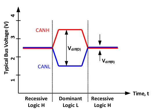 Figure 23. Bus States
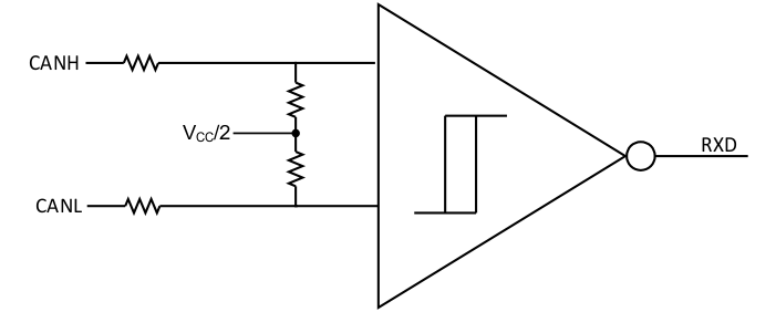 Figure 24. Simplified Recessive Common Mode Bias and Receiver
These CAN transceivers are typically used in applications with a host microprocessor or FPGA that includes the link layer portion of the CAN protocol. The different nodes on the network are typically connected through the use of a 120-Ω characteristic impedance twisted-pair cable with termination on both ends of the bus.
10.2 Typical Application
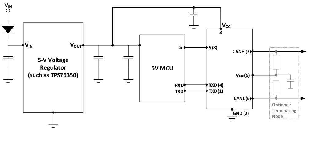 Figure 25. Typical Application Schematic
10.2.1 Design Requirements
10.2.1.1 Bus Loading, Length, and Number of Nodes
The ISO 11898 Standard specifies up to 1 Mbps data rate, maximum bus length of 40 meters, maximum drop line (stub) length of 0.3 meters and a maximum of 30 nodes. However, with careful network design, the system may have longer cables, longer stub lengths, and many more nodes to a bus. Many CAN organizations and standards have scaled the use of CAN for applications outside the original ISO 11898 standard. They have made system level trade-offs for data rate, cable length, and parasitic loading of the bus. Examples of some of these specifications are ARINC825, CANopen, CAN Kingdom, DeviceNet and NMEA200.
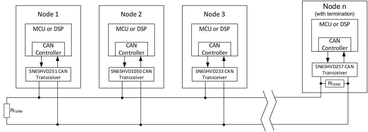 Figure 26. Typical CAN Bus
A high number of nodes requires a transceiver with high input impedance and wide common mode range such as the SN65HVD1050 CAN transceiver. ISO 11898-2 specifies the driver differential output with a 60-Ω load (two 120-Ω termination resistors in parallel) and the differential output must be greater than 1.5 V. The SN65HVD1050 device is specified to meet the 1.5-V requirement with a 60-Ω load, and additionally specified with a differential output voltage minimum of 1.2 V across a common mode range of –2 V to 7 V via a 330-Ω coupling network. This network represents the bus loading of 90 SN65HVD1050 transceivers based on their minimum differential input resistance of 30 kΩ. Therefore, the SN65HVD1050 supports up to 90 transceivers on a single bus segment with margin to the 1.2-V minimum differential input voltage requirement at each node.
For CAN network design, margin must be given for signal loss across the system and cabling, parasitic loadings, network imbalances, ground offsets and signal integrity thus a practical maximum number of nodes may be lower. Bus length may also be extended beyond the original ISO 11898 standard of 40 meters by careful system design and data rate tradeoffs. For example, CANopen network design guidelines allow the network to be up to 1-km with changes in the termination resistance, cabling, less than 64 nodes and significantly lowered data rate.
This flexibility in CAN network design is one of the key strengths of the various extensions and additional standards that have been built on the original ISO 11898 CAN standard.
10.2.1.2 CAN Termination
The ISO 11898 standard specifies the interconnect to be a twisted pair cable (shielded or unshielded) with 120-Ω characteristic impedance (ZO ). Resistors equal to the characteristic impedance of the line should be used to terminate both ends of the cable to prevent signal reflections. Unterminated drop lines (stubs) connecting nodes to the bus should be kept as short as possible to minimize signal reflections. The termination may be on the cable or in a node, but if nodes may be removed from the bus the termination must be carefully placed so that it is not removed from the bus.
Termination is typically a 120-Ω resistor at each end of the bus. If filtering and stabilization of the common mode voltage of the bus is desired, then split termination may be used (see Figure 27). Split termination uses two 60-Ω resistors with a capacitor in the middle of these resistors to ground. Split termination improves the electromagnetic emissions behavior of the network by eliminating fluctuations in the bus common mode voltages at the start and end of message transmissions.
Care should be taken when determining the power ratings of the termination resistors. A typical worst case fault condition is if the system power supply and ground were shorted across the termination resistance which would result in much higher current through the termination resistance than the CAN transceiver's current limit.
 Figure 27. CAN Termination
10.2.1.2.1 Loop Propagation Delay
Transceiver loop delay is a measure of the overall device propagation delay, consisting of the delay from the driver input (TXD pin) to the differential outputs (CANH and CANL pins), plus the delay from the receiver inputs (CANH and CANL) to its output (RXD pin). A typical loop delay for the SN65HVD1050 transceiver is displayed in Figure 29.
10.2.2 Detailed Design Procedure
10.2.2.1 ESD Protection
A typical application that employees a CAN bus network may require some form of ESD, burst, and surge protection to shield the CAN transceiver against unwanted transients that can potential damage the transceiver. To help shield the SN65HVD1050 transceiver against these high energy transients, transient voltage suppressors can be implemented on the CAN differential bus terminals. These devices will help absorb the impact of a ESD, burst, and/or surge strike.
10.2.2.2 Transient Voltage Suppresser (TVS) Diodes
Transient voltage suppressors are the preferred protection components for a CAN bus due to their low capacitance, which allows them to be designed into every node of a multi-node network without requiring a reduction in data rate. With response times of a few picoseconds and power ratings of up to several kilowatts, TVS diodes present the most effective protection against ESD, burst, and surge transients.
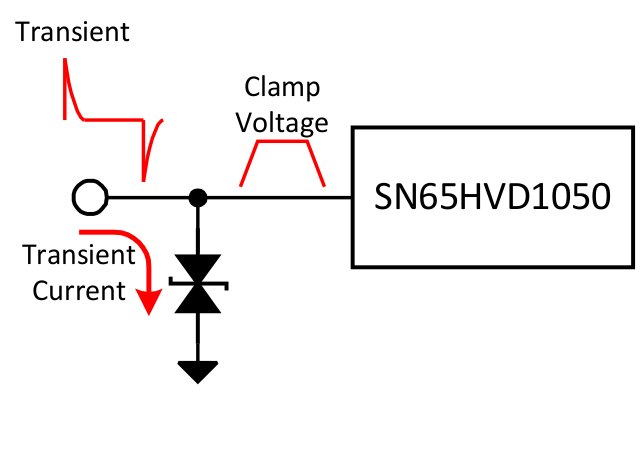 Figure 28. Effect of Transient Voltage Supressor
10.2.3 Application Curve
Figure 29 shows the typical loop delay for the SN65HVD1050.
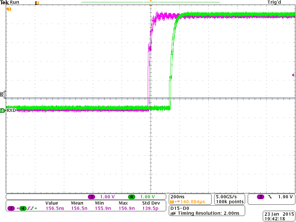 Figure 29. tLOOP Delay Waveform
10.3 System Example
10.3.1 ISO 11898 Compliance of SN65HVD1050 5-V CAN Transceiver
10.3.1.1 Introduction
The SN65HVD1050 CAN transceiver is a 5-V CAN transceiver that meets or exceeds the specification of the ISO 11898 standard for applications employing a controller area network.
10.3.1.2 Differential Signal
CAN is a differential bus where complementary signals are sent over two wires and the voltage difference between the two wires defines the logical state of the bus. The differential CAN receiver monitors this voltage difference and outputs the bus state with a single ended logic level output signal.
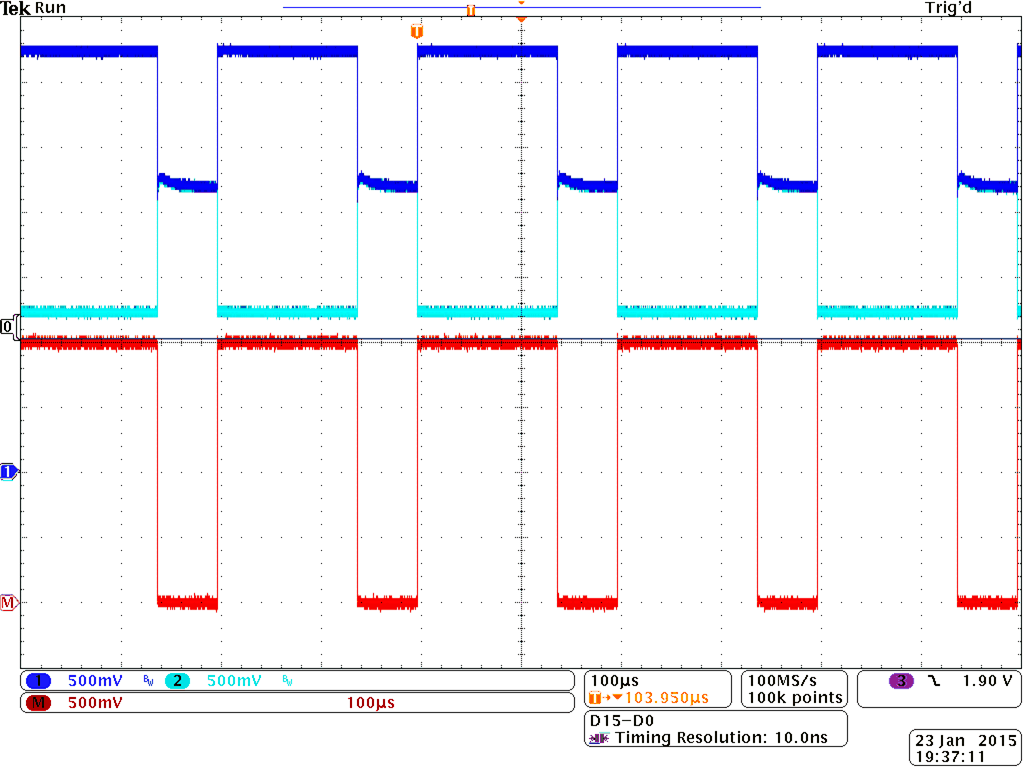 Figure 30. Differential Output Waveform
The CAN driver creates the differential voltage between CANH and CANL in the dominant state. The dominant differential output of the SN65HVD1050 is greater than 1.5 V and less than 3 V across a 60-Ω load as defined by the ISO 11898 standard. Figure 30 shows CANH, CANL, and the diferential dominanat state level for the SN65HVD1050.
A CAN receiver is required to output a recessive state when less than 500 mV of differential voltage exists on the bus, and a dominant state when more than 900 mV of differential voltage exists on the bus. The CAN receiver must do this with common-mode input voltages from –2 V to 7 V.
10.3.1.3 Common-Mode Signal
A common-mode signal is an average voltage of the two signal wires that the differential receiver rejects. The common-mode signal comes from the CAN driver, ground noise, and coupled bus noise. Because the bias voltage of the recessive state of the device is dependent on VCC, any noise present or variation of VCC will have an effect on this bias voltage seen by the bus. The SN65HVD1050 CAN transceiver has the recessive bias voltage set to 0.5 × VCC to comply with the ISO 11898-2 CAN standard.