SLLS632C December 2005 – February 2015 SN65HVD1050
PRODUCTION DATA.
- 1 Features
- 2 Applications
- 3 Description
- 4 Revision History
- 5 Description (Continued)
- 6 Pin Configuration and Functions
-
7 Specifications
- 7.1 Absolute Maximum Ratings
- 7.2 ESD Ratings
- 7.3 Recommended Operating Conditions
- 7.4 Thermal Information
- 7.5 Driver Electrical Characteristics
- 7.6 Receiver Electrical Characteristics
- 7.7 Device Switching Characteristics
- 7.8 Driver Switching Characteristics
- 7.9 Receiver Switching Characteristics
- 7.10 Supply Current
- 7.11 S-Pin Characteristics
- 7.12 VREF-Pin Characteristics
- 7.13 Typical Characteristics
- 8 Parameter Measurement Information
- 9 Detailed Description
- 10Application and Implementation
- 11Power Supply Recommendations
- 12Layout
- 13Device and Documentation Support
- 14Mechanical, Packaging, and Orderable Information
8 Parameter Measurement Information


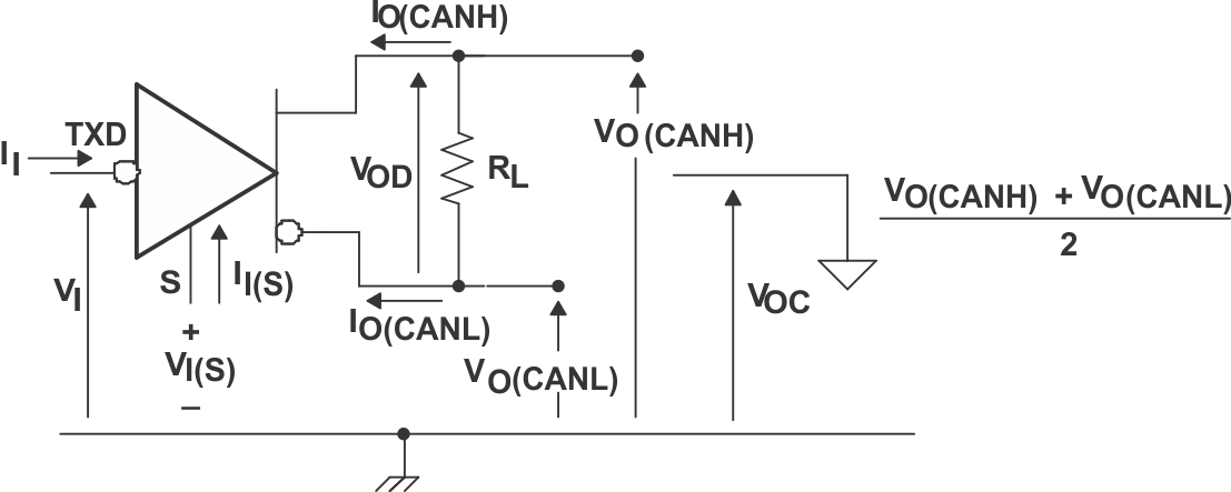
 Figure 14. Driver Test Circuit and Voltage Waveforms
 Figure 15. Receiver Voltage and Current Definitions

A. The input pulse is supplied by a generator having the following characteristics: PRR ≤ 125 kHz, 50% duty cycle, tr ≤ 6 ns, tf ≤ 6ns, ZO = 50 Ω.
B. CL includes instrumentation and fixture capacitance within ±20%.
Figure 16. Receiver Test Circuit and Voltage Waveforms
Table 1. Differential Input Voltage Threshold Test
| INPUT | OUTPUT | |||
|---|---|---|---|---|
| VCANH | VCANL | |VID| | R | |
| –11.1V | –12V | 900 mV | L | VOL |
| 12V | 11.1V | 900 mV | L | |
| –6V | –12V | 6V | L | |
| 12V | 6V | 6V | L | |
| –11.5V | –12V | 500 mV | H | VOH |
| 12V | 11.5V | 500 mV | H | |
| –12V | –6V | 6V | H | |
| 6V | 12V | 6V | H | |
| Open | Open | X | H | |
 Figure 17. TEN Test Circuit and Waveform

NOTE:
All VI input pulses are from 0V to VCC and supplied by a generator having the following characteristics: tr or tf ≤ 6 ns. Pulse Repetition Rate (PRR) = 125 kHz, 50% duty cycle.
A. All VI input pulses are from 0V to VCC and supplied by a generator having the following characteristics: tr or tf ≤ 6 ns. Pulse Repetition Rate (PRR) = 125 kHz, 50% duty cycle.
Figure 19. T(LOOP) Test Circuit and Waveform

A. All VI input pulses are from 0 V to VCC and supplied by a generator having the following characteristics: tr or tf ≤ 6 ns. Pulse Repetition Rate (PRR) = 500 Hz, 50% duty cycle.
B. CL = 100 pF includes instrumentation and fixture capacitance within ±20%.
Figure 20. Dominant Time-Out Test Circuit and Waveforms
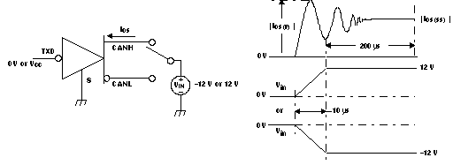
 Figure 21. Driver Short-Circuit Current Test and Waveform