SLLS934F November 2008 – November 2015 SN65HVD11-HT
PRODUCTION DATA.
- 1 Features
- 2 Applications
- 3 Description
- 4 Revision History
- 5 Pin Configuration and Functions
- 6 Specifications
- 7 Parameter Measurement Information
- 8 Detailed Description
- 9 Application and Implementation
- 10Power Supply Recommendations
- 11Layout
- 12Device and Documentation Support
- 13Mechanical, Packaging, and Orderable Information
封装选项
机械数据 (封装 | 引脚)
散热焊盘机械数据 (封装 | 引脚)
订购信息
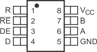
5 Pin Configuration and Functions
D, JD, or HKJ Package
8-Pin SOIC, PDIP, or CFP
Top View

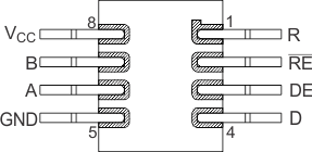
HKQ Package
8-Pin CFP
Top View

Pin Functions
| PIN | TYPE | DESCRIPTION | ||
|---|---|---|---|---|
| NAME | SOIC, PDIP |
HKQ | ||
| A | 6 | 6 | Bus input/output | Driver output or receiver input (complementary to B) |
| B | 7 | 7 | Bus input/output | Driver output or receiver input (complementary to A) |
| D | 4 | 4 | Digital input | Driver data input |
| DE | 3 | 3 | Digital input | Active-high driver enable |
| GND | 5 | 5 | Reference potential | Local device ground |
| R | 1 | 1 | Digital output | Receive data output |
| RE | 2 | 2 | Digital input | Active-low receiver enable |
| VCC | 8 | 8 | Supply | 3-V to 3.6-V supply |
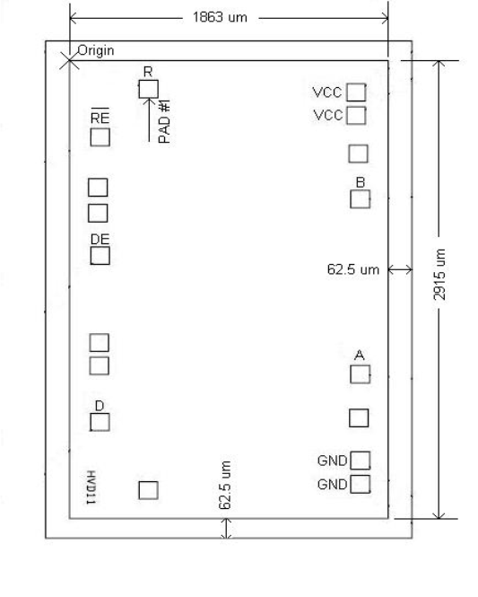
Bare Die Information
| DIE THICKNESS | BACKSIDE FINISH | BACKSIDE POTENTIAL | BOND PAD METALLIZATION COMPOSITION |
|---|---|---|---|
| 15 mils. | Silicon with backgrind | GND | Cu-Ni-Pd |
Bond Pad Coordinates in Microns - Rev A
| DESCRIPTION(1) | PAD NUMBER | a | b | c | d |
|---|---|---|---|---|---|
| R | 1 | 69.3 | 372.15 | 185.3 | 489.15 |
| ~RE | 2 | 388.75 | 71.5 | 503.75 | 186.5 |
| DNC | 3 | 722.4 | 55.4 | 839.4 | 172.4 |
| DNC | 4 | 891.4 | 55.4 | 1008.4 | 172.4 |
| DE | 5 | 1174.8 | 71.5 | 1289.8 | 186.5 |
| DNC | 6 | 1754.35 | 65.4 | 1869.35 | 180.4 |
| DNC | 7 | 1907.35 | 65.4 | 2022.35 | 180.4 |
| D | 8 | 2280.55 | 69.5 | 2395.55 | 184.5 |
| DNC | 9 | 2733.5 | 371.5 | 2848.5 | 486.5 |
| GND | 10 | 2691 | 1693.1 | 2808 | 1810.1 |
| GND | 11 | 2535 | 1693.1 | 2652 | 1810.1 |
| DNC | 12 | 2253.45 | 1685.65 | 2368.45 | 1800.65 |
| A | 13 | 1961.55 | 1693.1 | 2078.55 | 1810.1 |
| B | 14 | 799.55 | 1693.1 | 916.55 | 1810.1 |
| DNC | 15 | 498.35 | 1681.2 | 613.35 | 1796.2 |
| VCC | 16 | 244.8 | 1668.5 | 359.8 | 1783.5 |
| VCC | 17 | 91.8 | 1668.5 | 206.8 | 1783.5 |
(1) DNC = Do Not Connect
