ZHCSRD4I July   2003  – January 2023 SN65HVD1176 , SN75HVD1176

PRODUCTION DATA  

  1. 特性
  2. 应用
  3. 说明
  4. Revision History
  5. Pin Configuration and Functions
    1.     Pin Functions
  6. Specifications
    1. 6.1 Absolute Maximum Ratings
    2. 6.2 ESD Ratings
    3. 6.3 Recommended Operating Conditions
    4. 6.4 Thermal Information
    5. 6.5 Electrical Characteristics
    6. 6.6 Supply Current
    7. 6.7 Power Dissipation
    8. 6.8 Switching Characteristics
    9. 6.9 Typical Characteristics
      1.      Parameter Measurement Information
  7. Detailed Description
    1. 7.1 Overview
    2. 7.2 Functional Block Diagram
    3. 7.3 Feature Description
    4. 7.4 Device Functional Modes
  8. Application and Implementation
    1. 8.1 Application Information
    2. 8.2 Typical Application
      1. 8.2.1 Design Requirements
        1. 8.2.1.1 Data Rate and Bus Length
        2. 8.2.1.2 Stub Length
        3. 8.2.1.3 Bus Loading
        4. 8.2.1.4 Receiver Failsafe
      2. 8.2.2 Detailed Design Procedure
      3. 8.2.3 Application Curve
  9. Power Supply Recommendations
  10. 10Layout
    1. 10.1 Layout Guidelines
    2. 10.2 Layout Example
  11. 11Device and Documentation Support
    1. 11.1 第三方米6体育平台手机版_好二三四免责声明
    2. 11.2 Documentation Support
    3. 11.3 Related Links
    4. 11.4 支持资源
    5. 11.5 Trademarks
    6. 11.6 静电放电警告
    7. 11.7 术语表
  12. 12Mechanical, Packaging, and Orderable Information

封装选项

机械数据 (封装 | 引脚)
散热焊盘机械数据 (封装 | 引脚)
订购信息

Device Functional Modes

Table 7-1 Driver Function Table(1)
INPUTENABLEOUTPUTS
DDEAB
HHHL
LHLH
XLZZ
XOPENZZ
OPENHHL
H = high level, L = low level, X = don’t care,
Z = high impedance (off)
Table 7-2 Receiver Function Table(1)
DIFFRENTIAL INPUT
VID = (VA – VB)
ENABLE
RE
OUTPUT
R
VID ≥ –0.02 VLH
–0.2 V < VID < –0.02 VL?
VID ≤ –0.2 VLL
XHZ
XOPENZ
Open CircuitLH
Short CircuitLH
Idle (terminated) busLH
H = high level, L = low level, X = don’t care,
Z = high impedance (off), ? = indeterminate
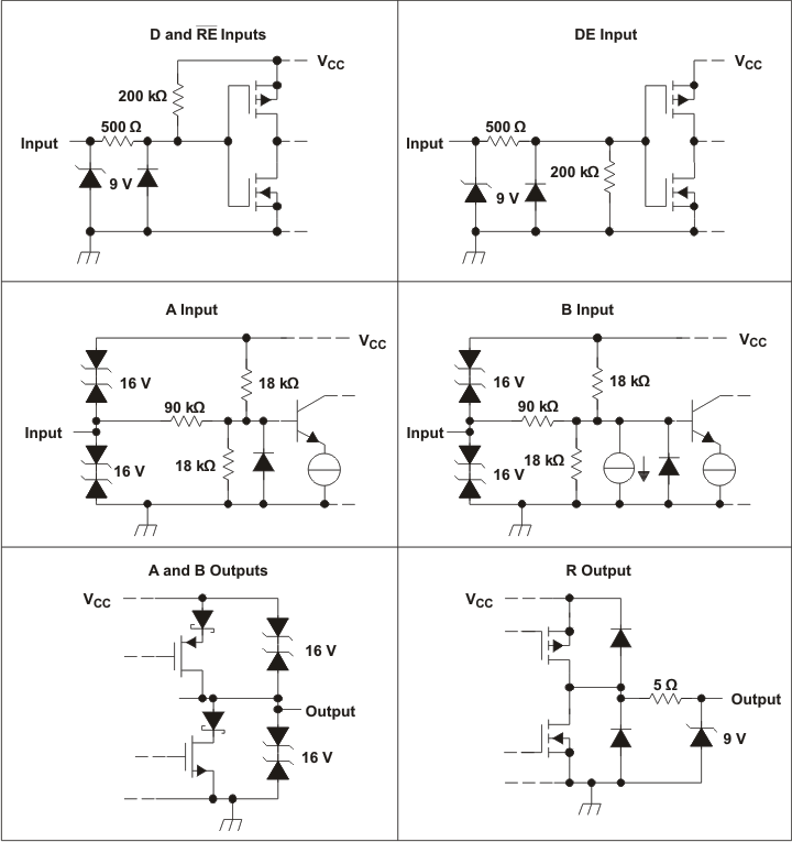
GUID-170FBB6E-3507-413C-8215-61586F754735-low.gifFigure 7-2 Equivalent Input and Output Schematic Diagrams