SLLS877H December 2007 – March 2017 SN65HVD1780 , SN65HVD1781 , SN65HVD1782
PRODUCTION DATA.
- 1 Features
- 2 Applications
- 3 Description
- 4 Revision History
- 5 Device Comparison Table
- 6 Pin Configuration and Functions
- 7 Specifications
- 8 Parameter Measurement Information
- 9 Detailed Description
- 10Application and Implementation
- 11Power Supply Recommendations
- 12Layout
- 13Device and Documentation Support
- 14Mechanical, Packaging, and Orderable Information
10 Application and Implementation
NOTE
Information in the following applications sections is not part of the TI component specification, and TI does not warrant its accuracy or completeness. TI’s customers are responsible for determining suitability of components for their purposes. Customers should validate and test their design implementation to confirm system functionality.
10.1 Application Information
The SN65HVD178x devices are half-duplex RS-485 transceivers commonly used for asynchronous data transmissions. The driver and receiver enable pins allow for the configuration of different operating modes.
 Figure 15. Half-Duplex Transceiver Configurations
Using independent enable lines provides the most flexible control as it allows for the driver and the receiver to be turned on and off individually. While this configuration requires two control lines, it allows for selective listening into the bus traffic, whether the driver is transmitting data or not.
Combining the enable signals simplifies the interface to the controller by forming a single direction-control signal. In this configuration, the transceiver operates as a driver when the direction-control line is high, and as a receiver when the direction-control line is low.
Additionally, only one line is required when connecting the receiver-enable input to ground and controlling only the driver-enable input. In this configuration, a node not only receives the data from the bus, but also the data it sends and can verify that the correct data have been transmitted.
10.2 Typical Application
An RS-485 bus consists of multiple transceivers connecting in parallel to a bus cable. To eliminate line reflections, each cable end is terminated with a termination resistor, RT, whose value matches the characteristic impedance, Z0, of the cable. This method, known as parallel termination, allows for higher data rates over longer cable length.
 Figure 16. Typical RS-485 Network With Half-Duplex Transceivers
10.2.1 Design Requirements
RS-485 is a robust electrical standard suitable for long-distance networking that may be used in a wide range of applications with varying requirements, such as distance, data rate, and number of nodes.
10.2.1.1 Data Rate and Bus Length
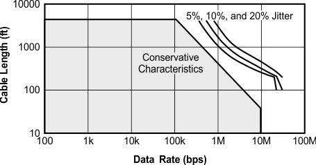
There is an inverse relationship between data rate and bus length, meaning the higher the data rate, the shorter the cable length; and conversely, the lower the data rate, the longer the cable may be without introducing data errors. While most RS-485 systems use data rates from 10 kbps to 100 kbps, some applications require data rates up to 250 kbps at distances of 4000 feet and longer. Longer distances are possible by allowing for small signal jitter of up to 5% or 10%.
 Figure 17. Cable Length vs Data Rate Characteristic
Even higher data rates are achievable (for example, 10 Mbps for the SN65HVD1782) in cases where the interconnect is short enough (or has suitably low attenuation at signal frequencies) to not degrade the data.
10.2.1.2 Stub Length
When connecting a node to the bus, the distance between the transceiver inputs and the cable trunk, known as the stub, should be as short as possible. Stubs present a non-terminated piece of bus line which can introduce reflections as the length of the stub increases. As a general guideline, the electrical length, or round-trip delay, of a stub should be less than one-tenth of the rise time of the driver, thus giving a maximum physical stub length as shown in Equation 1.
where
- tr is the 10/90 rise time of the driver
- c is the speed of light (3 × 10⁸ m/s)
- v is the signal velocity of the cable or trace as a factor of c
10.2.1.3 Bus Loading
The RS-485 standard specifies that a compliant driver must be able to driver 32 unit loads (UL), where 1 unit load represents a load impedance of approximately 12 kΩ. The SN65HVD1780 and SN65HVD1781 are 1/10 unit load transceivers, and so up to 320 can be placed on a common bus. The SN65HVD1782 is a 1/2 unit load transceiver, so up to 64 can share a bus.
10.2.1.4 Receiver Failsafe
The differential receivers of the SN65HVD178x family are “failsafe” to invalid bus states caused by:
- Open bus conditions, such as a disconnected connector
- Shorted bus conditions, such as cable damage shorting the twisted-pair together
- Idle bus conditions that occur when no driver on the bus is actively driving
In any of these cases, the differential receiver will output a failsafe logic High state so that the output of the receiver is not indeterminate.
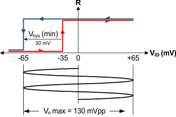
Receiver failsafe is accomplished by offsetting the receiver thresholds such that the “input indeterminate” range does not include zero volts differential. To comply with the RS-422 and RS-485 standards, the receiver output must output a High when the differential input VID is more positive than +200 mV, and must output a Low when VID is more negative than –200 mV. The receiver parameters which determine the failsafe performance are VIT(+), VIT(-), and VHYS (the separation between VIT(+) and VIT(-)). As shown in the Electrical Characteristics, differential signals more negative than –200 mV will always cause a Low receiver output, and differential signals more positive than +200 mV will always cause a High receiver output.
When the differential input signal is close to zero, it is still above the maximum VIT(+) threshold of –35 mV, and the receiver output will be High. Only when the differential input is more than VHYS below VIT(+) will the receiver output transition to a Low state. Therefore, the noise immunity of the receiver inputs during a bus fault condition includes the receiver hysteresis value, VHYS, as well as the value of VIT(+).
 Figure 18. SN65HVD178x Noise Immunity Under Bus Fault Conditions
10.2.2 Detailed Design Procedure
10.2.2.1 Custom Design with WEBENCH® Tools
Click here to create a custom design using the SN65HVD178x device with the WEBENCH® Power Designer.
- Start by entering your VIN, VOUT, and IOUT requirements.
- Optimize your design for key parameters like efficiency, footprint and cost using the optimizer dial and compare this design with other possible solutions from Texas Instruments.
- The WEBENCH Power Designer provides you with a customized schematic along with a list of materials with real time pricing and component availability.
- In most cases, you will also be able to:
- Run electrical simulations to see important waveforms and circuit performance
- Run thermal simulations to understand the thermal performance of your board
- Export your customized schematic and layout into popular CAD formats
- Print PDF reports for the design, and share your design with colleagues
- Get more information about WEBENCH tools at www.ti.com/WEBENCH.
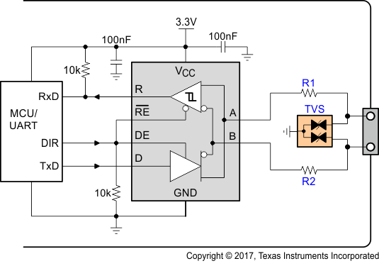
Although the SN65HVD178x family is internally protected against human-body-model ESD strikes up to 16 kV, additional protection against higher-energy transients can be provided at the application level by implementing external protection devices.
 Figure 19. RS-485 Transceiver With External Transient Protection
Figure 19 shows a protection circuit intended to withstand 8-kV IEC ESD (per IEC 61000-4-2) as well as 4-kV EFT (per IEC 61000-4-4).
Table 4. Bill of Materials
| DEVICE | FUNCTION | ORDER NUMBER | MANUFACTURER |
|---|---|---|---|
| XCVR | RS-485 Transceiver | SN65HVD1781 | TI |
| R1,R2 | 10 Ω, Pulse-Proof Thick-Film Resistor | CRCW0603010RJNEAHP | Vishay |
| TVS | Bidirectional 600-W Transient Suppressor | SMBJ43CA | Littelfuse |
10.2.3 Application Curve
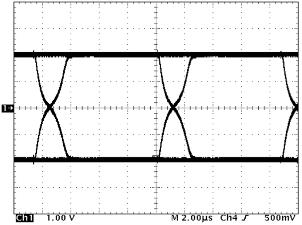
 Figure 20. SN65HVD1780 Differential Output at 115 kbps