SLLS877H December 2007 – March 2017 SN65HVD1780 , SN65HVD1781 , SN65HVD1782
PRODUCTION DATA.
- 1 Features
- 2 Applications
- 3 Description
- 4 Revision History
- 5 Device Comparison Table
- 6 Pin Configuration and Functions
- 7 Specifications
- 8 Parameter Measurement Information
- 9 Detailed Description
- 10Application and Implementation
- 11Power Supply Recommendations
- 12Layout
- 13Device and Documentation Support
- 14Mechanical, Packaging, and Orderable Information
7 Specifications
7.1 Absolute Maximum Ratings(1)
(1) Stresses beyond those listed under Absolute Maximum Ratings may cause permanent damage to the device. These are stress ratings only and functional operation of the device at these or any other conditions beyond those indicated under Recommended Operating Conditions is not implied. Exposure to absolute-maximum-rated conditions for extended periods may affect device reliability.
7.2 ESD Ratings: JEDEC
| VALUE | UNIT | ||||
|---|---|---|---|---|---|
| V(ESD) | Electrostatic discharge | Human body model (HBM), per ANSI/ESDA/JEDEC JS-001, all pins(1) | Bus pins and GND | ±16000 | V |
| All pins | ±4000 | ||||
| Charged device model (CDM), per JEDEC specification JESD22-C101, all pins(2) | ±2000 | ||||
| Machine model JEDEC Standard 22, Test Method A115, all pins | ±400 | V | |||
(1) JEDEC document JEP155 states that 500-V HBM allows safe manufacturing with a standard ESD control process.
(2) JEDEC document JEP157 states that 250-V CDM allows safe manufacturing with a standard ESD control process.
7.3 ESD Ratings: IEC
| VALUE | UNIT | |||
|---|---|---|---|---|
| V(ESD) | Electrostatic discharge | IEC 60749-26 ESD (human body model), bus terminals and GND | ±16000 | V |
7.4 Recommended Operating Conditions
| MIN | NOM | MAX | UNIT | |||
|---|---|---|---|---|---|---|
| VCC | Supply voltage | 3.15 | 5 | 5.5 | V | |
| VI | Input voltage at any bus terminal (separately or common mode)(1) | –7 | 12 | V | ||
| VIH | High-level input voltage (driver, driver enable, and receiver enable inputs) | 2 | VCC | V | ||
| VIL | Low-level input voltage (driver, driver enable, and receiver enable inputs) | 0 | 0.8 | V | ||
| VID | Differential input voltage | –12 | 12 | V | ||
| IO | Output current, driver | –60 | 60 | mA | ||
| Output current, receiver | –8 | 8 | mA | |||
| RL | Differential load resistance | 54 | 60 | Ω | ||
| CL | Differential load capacitance | 50 | pF | |||
| 1/tUI | Signaling rate | SN65HVD1780 | 115 | kbps | ||
| SN65HVD1781 | 1 | Mbps | ||||
| SN65HVD1782 | 10 | |||||
| TA | Operating free-air temperature (See Power Dissipation Characteristics) | 5-V supply | –40 | 105 | °C | |
| 3.3-V supply | –40 | 125 | ||||
| TJ | Junction temperature | –40 | 150 | °C | ||
(1) By convention, the least positive (most negative) limit is designated as minimum in this data sheet.
7.5 Thermal Information
| THERMAL METRIC(1) | SN65HVD178x | UNIT | |||
|---|---|---|---|---|---|
| D (SOIC) | P (PDIP) | ||||
| 8 PINS | 8 PINS | ||||
| RθJA | Junction-to-ambient thermal resistance | JEDEC high-K model | 138 | 59 | °C/W |
| JEDEC low-K model | 242 | 128 | |||
| RθJC(top) | Junction-to-case (top) thermal resistance | 61 | 61 | °C/W | |
| RθJB | Junction-to-board thermal resistance | 62 | 39 | °C/W | |
| ψJT | Junction-to-top characterization parameter | 3.4 | 17.6 | °C/W | |
| ψJB | Junction-to-board characterization parameter | 33.4 | 28.3 | °C/W | |
| RθJC(bot) | Junction-to-case (bottom) thermal resistance | N/A | N/A | °C/W | |
(1) For more information about traditional and new thermal metrics, see the Semiconductor and IC Package Thermal Metrics application report.
7.6 Electrical Characteristics
over operating free-air temperature range (unless otherwise noted)| PARAMETER | TEST CONDITIONS | MIN | TYP | MAX | UNIT | |||
|---|---|---|---|---|---|---|---|---|
| |VOD| | Driver differential output voltage magnitude | RL = 60 Ω, 4.75 V ≤ VCC 375 Ω on each output to –7 V to 12 V Figure 6 |
TA < 85°C | 1.5 | V | |||
| TA < 125°C | 1.4 | |||||||
| RL = 54 Ω, 4.75 V ≤ VCC ≤ 5.25 V |
TA < 85°C | 1.7 | 2 | |||||
| TA < 125°C | 1.5 | |||||||
| RL = 54 Ω, 3.15 V ≤ VCC ≤ 3.45 V |
0.8 | 1 | ||||||
| RL = 100 Ω, 4.75 V ≤ VCC ≤ 5.25 V |
TA < 85°C | 2.2 | 2.5 | |||||
| TA < 125°C | 2 | |||||||
| Δ|VOD| | Change in magnitude of driver differential output voltage | RL = 54 Ω | –50 | 0 | 50 | mV | ||
| VOC(SS) | Steady-state common-mode output voltage | 1 | VCC/2 | 3 | V | |||
| ΔVOC | Change in differential driver output common-mode voltage | –50 | 0 | 50 | mV | |||
| VOC(PP) | Peak-to-peak driver common-mode output voltage | Center of two 27-Ω load resistors See Figure 7 |
500 | mV | ||||
| COD | Differential output capacitance | 23 | pF | |||||
| VIT+ | Positive-going receiver differential input voltage threshold | –100 | –35 | mV | ||||
| VIT– | Negative-going receiver differential input voltage threshold | –180 | –150 | mV | ||||
| VHYS | Receiver differential input voltage threshold hysteresis (VIT+ – VIT–) | 30 | 50 | mV | ||||
| VOH | Receiver high-level output voltage | IOH = –8 mA | 2.4 | VCC – 0.3 | V | |||
| VOL | Receiver low-level output voltage | IOL = 8 mA | TA < 85°C | 0.2 | 0.4 | V | ||
| TA < 125°C | 0.5 | |||||||
| II(LOGIC) | Driver input, driver enable, and receiver enable input current | –50 | 50 | μA | ||||
| IOZ | Receiver output high-impedance current | VO = 0 V or VCC, RE at VCC | –1 | 1 | μA | |||
| IOS | Driver short-circuit output current | –200 | 200 | mA | ||||
| II(BUS) | Bus input current (disabled driver) | VCC = 3.15 to 5.5 V or VCC = 0 V, DE at 0 V |
VI = 12 V | 1780, 1781 | 75 | 100 | μA | |
| 1782 | 400 | 500 | ||||||
| VI = –7 V | 1780, 1781 | –60 | –40 | |||||
| 1782 | –400 | –300 | ||||||
| ICC | Supply current (quiescent) | Driver and receiver enabled | DE = VCC, RE = GND, no load |
4 | 6 | mA | ||
| Driver enabled, receiver disabled | DE = VCC, RE = VCC, no load |
3 | 5 | |||||
| Driver disabled, receiver enabled | DE = GND, RE = GND, no load |
2 | 4 | |||||
| Drive and receiver disabled (standby mode) | DE = GND, D = open, RE = VCC, no load, TA < 85°C |
0.15 | 1 | µA | ||||
| DE = GND, D = open, RE = VCC, no load, TA < 125°C |
12 | |||||||
| Supply current (dynamic) | See Typical Characteristics | |||||||
7.7 Power Dissipation Characteristics
over operating free-air temperature range (unless otherwise noted)| PARAMETER | TEST CONDITIONS | MAX | UNIT | ||
|---|---|---|---|---|---|
| PD | Power dissipation | VCC = 5.5 V, TJ = 150°C, RL = 300 Ω, CL = 50 pF (driver), CL = 15 pF (receiver) 5-V supply, unterminated(1) |
290 | mW | |
| VCC = 5.5 V, TJ = 150°C, RL = 100 Ω, CL = 50 pF (driver), CL = 15 pF (receiver) 5-V supply, RS-422 load(1) |
320 | ||||
| VCC = 5.5 V, TJ = 150°C, RL = 54 Ω, CL = 50 pF (driver), CL = 15 pF (receiver) 5-V supply, RS-485 load(1) |
400 | ||||
| TSD | Thermal-shutdown junction temperature | 170 | °C | ||
(1) Driver and receiver enabled, 50% duty cycle square-wave signal at signaling rate: 1 Mbps.
7.8 Switching Characteristics
over recommended operating conditions (unless otherwise noted)| PARAMETER | TEST CONDITIONS | MIN | TYP | MAX | UNIT | ||
|---|---|---|---|---|---|---|---|
| DRIVER (SN65HVD1780) | |||||||
| tr, tf | Driver differential output rise or fall time | RL = 54 Ω, CL = 50 pF, See Figure 8 |
3.15 V < VCC < 3.45 V | 0.4 | 1.4 | 1.8 | µs |
| 3.15 V < VCC < 5.5 V | 0.4 | 1.7 | 2.6 | ||||
| tPHL, tPLH | Driver propagation delay | RL = 54 Ω, CL = 50 pF, See Figure 8 |
0.8 | 2 | µs | ||
| tSK(P) | Driver differential output pulse skew, |tPHL – tPLH| |
RL = 54 Ω, CL = 50 pF, See Figure 8 |
20 | 250 | ns | ||
| tPHZ, tPLZ | Driver disable time | See Figure 9 and Figure 10 | 0.1 | 5 | µs | ||
| tPZH, tPZL | Driver enable time | Receiver enabled | See Figure 9 and Figure 10 | 0.2 | 3 | µs | |
| Receiver disabled | See Figure 9 and Figure 10 | 3 | 12 | ||||
| DRIVER (SN65HVD1781) | |||||||
| tr, tf | Driver differential output rise or fall time | RL = 54 Ω, CL = 50 pF, See Figure 8 | 50 | 300 | ns | ||
| tPHL, tPLH | Driver propagation delay | RL = 54 Ω, CL = 50 pF, See Figure 8 | 200 | ns | |||
| tSK(P) | Driver differential output pulse skew, |tPHL – tPLH| |
RL = 54 Ω, CL = 50 pF, See Figure 8 | 25 | ns | |||
| tPHZ, tPLZ | Driver disable time | See Figure 9 and Figure 10 | 3 | µs | |||
| tPZH, tPZL | Driver enable time | Receiver enabled | See Figure 9 and Figure 10 | 300 | ns | ||
| Receiver disabled | See Figure 9 and Figure 10 | 10 | µs | ||||
| DRIVER (SN65HVD1782) | |||||||
| tr, tf | Driver differential output rise or fall time | RL = 54 Ω, CL = 50 pF |
All VCC and Temperature | 50 | ns | ||
| VCC > 4.5 V and T < 105°C |
16 | ||||||
| tPHL, tPLH | Driver propagation delay | RL = 54 Ω, CL = 50 pF |
See Figure 8 | 55 | ns | ||
| tSK(P) | Driver differential output pulse skew, |tPHL – tPLH| |
RL = 54 Ω, CL = 50 pF |
See Figure 8 | 10 | ns | ||
| tPHZ, tPLZ | Driver disable time | See Figure 9 and Figure 10 | 3 | µs | |||
| tPZH, tPZL | Driver enable time | Receiver enabled | See Figure 9 and Figure 10 | 300 | ns | ||
| Receiver disabled | See Figure 9 and Figure 10 | 9 | µs | ||||
| RECEIVER | |||||||
| tr, tf | Receiver output rise or fall time | CL = 15 pF, See Figure 11 |
All devices | 4 | 15 | ns | |
| tPHL, tPLH | Receiver propagation delay time | CL = 15 pF, See Figure 11 |
SN65HVD1780, SN65HVD1781 |
100 | 200 | ns | |
| SN65HVD1782 | 80 | ||||||
| tSK(P) | Receiver output pulse skew, |tPHL – tPLH| |
CL = 15 pF, See Figure 11 |
SN65HVD1780, SN65HVD1781 |
6 | 20 | ns | |
| SN65HVD1782 | 5 | ||||||
| tPLZ, tPHZ | Receiver disable time | Driver enabled, See Figure 12 | 15 | 100 | ns | ||
| tPZL(1), tPZH(1)
tPZL(2), tPZH(2) |
Receiver enable time | Driver enabled, See Figure 12 | 80 | 300 | ns | ||
| Driver disabled, See Figure 13 | 3 | 9 | μs | ||||
7.9 Typical Characteristics
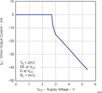 Figure 1. Driver Output Current vs Supply Voltage
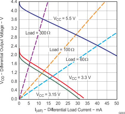 Figure 3. Differential Output Voltage vs Differential Load Current
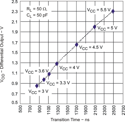 Figure 5. SN65HVD1780 Differential Output Amplitude and Transition Time vs Supply Voltage
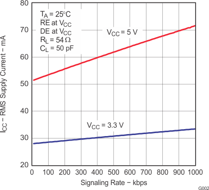 Figure 2. RMS Supply Current vs Signaling Rate
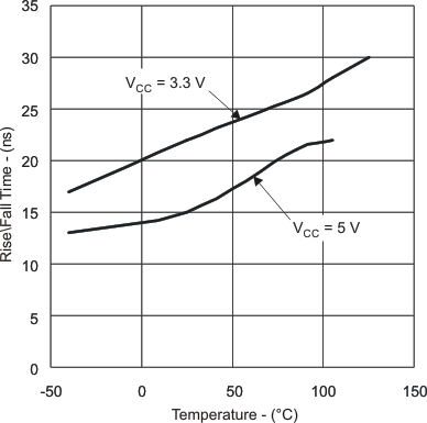 Figure 4. SN65HVD1782 Rise or Fall Time