ZHCSR19G December 2002 – September 2022 SN65HVD20 , SN65HVD21 , SN65HVD22 , SN65HVD23 , SN65HVD24
PRODUCTION DATA
- 1 特性
- 2 应用
- 3 说明
- 4 Revision History
- 5 说明(续)
- 6 Device Comparison
- 7 Pin Configuration and Functions
-
8 Specifications
- 8.1 Absolute Maximum Ratings
- 8.2 ESD Ratings
- 8.3 Recommended Operating Conditions
- 8.4 Thermal Information
- 8.5 Driver Electrical Characteristics
- 8.6 Receiver Electrical Characteristics
- 8.7 Driver Switching Characteristics
- 8.8 Receiver Switching Characteristics
- 8.9 Receiver Equalization Characteristics
- 8.10 Power Dissipation
- 8.11 Typical Characteristics
- 9 Parameter Measurement Information
- 10Detailed Description
- 11Application and Implementation
- 12Power Supply Recommendations
- 13Layout
- 14Device and Documentation Support
- 15Mechanical, Packaging, and Orderable Information
10.4 Device Functional Modes
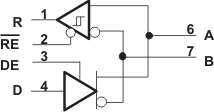
The driver and receiver behavior for different input conditions are shown in Table 10-1 and Table 10-2, respectively.
Table 10-1 Driver Function Table(1)
| DEVICE | INPUT | ENABLE | OUTPUTS | |
|---|---|---|---|---|
| D | DE | A | B | |
| SN65HVD2[0,1,2] | H | H | H | L |
| L | H | L | H | |
| X | L | Z | Z | |
| X | OPEN | Z | Z | |
| OPEN | H | H | L | |
| SN65HVD2[3,4] | H | H | H | L |
| L | H | L | H | |
| X | L | Z | Z | |
| X | OPEN | Z | Z | |
| OPEN | H | L | H | |
(1) Legend: H = high level, L = low level, X = don’t care, Z = high impedance (off), ? = indeterminate
Table 10-2 Receiver Function Table(1)
| DIFFERENTIAL INPUT VID = (VA – VB) | ENABLE RE | OUTPUT R |
|---|---|---|
| 0.2 V ≤ VID | L | H |
| –0.2 V < VID < 0.2 V | L | H(2) |
| VID ≤ –0.2 V | L | L |
| X | H | Z |
| X | OPEN | Z |
| Open circuit | L | H |
| Short Circuit | L | H |
| Idle (terminated) bus | L | H |
(1) H = high level, L = low level, Z = high impedance (off)
(2) If the differential input VID remains within the transition range for more than 250 µs, the integrated failsafe circuitry detects a bus fault, and set the receiver output to a high state. See Figure 9-15.
 Figure 10-3 Logic Diagram