ZHCSDL3O MARCH   2001  – April 2018 SN65HVD230 , SN65HVD231 , SN65HVD232

PRODUCTION DATA.  

  1. 特性
  2. 应用
  3. 说明
    1.     Device Images
      1.      等效输入和输出原理图
  4. 修订历史记录
  5. 说明 (续)
  6. Device Comparison Table
  7. Pin Configuration and Functions
    1.     Pin Functions
  8. Specifications
    1. 8.1  Absolute Maximum Ratings
    2. 8.2  ESD Ratings
    3. 8.3  Recommended Operating Conditions
    4. 8.4  Thermal Information
    5. 8.5  Electrical Characteristics: Driver
    6. 8.6  Electrical Characteristics: Receiver
    7. 8.7  Switching Characteristics: Driver
    8. 8.8  Switching Characteristics: Receiver
    9. 8.9  Switching Characteristics: Device
    10. 8.10 Device Control-Pin Characteristics
    11. 8.11 Typical Characteristics
  9. Parameter Measurement Information
  10. 10Detailed Description
    1. 10.1 Overview
    2. 10.2 Functional Block Diagram
    3. 10.3 Feature Description
      1. 10.3.1 Vref Voltage Reference
      2. 10.3.2 Thermal Shutdown
    4. 10.4 Device Functional Modes
      1. 10.4.1 High-Speed Mode
      2. 10.4.2 Slope Control Mode
      3. 10.4.3 Standby Mode (Listen Only Mode) of the HVD230
      4. 10.4.4 The Babbling Idiot Protection of the HVD230
      5. 10.4.5 Sleep Mode of the HVD231
      6. 10.4.6 Summary of Device Operating Modes
  11. 11Application and Implementation
    1. 11.1 Application Information
      1. 11.1.1 CAN Bus States
    2. 11.2 Typical Application
      1. 11.2.1 Design Requirements
        1. 11.2.1.1 CAN Termination
        2. 11.2.1.2 Loop Propagation Delay
        3. 11.2.1.3 Bus Loading, Length and Number of Nodes
      2. 11.2.2 Detailed Design Procedure
        1. 11.2.2.1 Transient Protection
        2. 11.2.2.2 Transient Voltage Suppressors
      3. 11.2.3 Application Curve
    3. 11.3 System Example
      1. 11.3.1 ISO 11898 Compliance of SN65HVD23x Family of 3.3 V CAN Transceivers
        1. 11.3.1.1 Introduction
        2. 11.3.1.2 Differential Signal
          1. 11.3.1.2.1 Common Mode Signal
        3. 11.3.1.3 Interoperability of 3.3-V CAN in 5-V CAN Systems
  12. 12Power Supply Recommendations
  13. 13Layout
    1. 13.1 Layout Guidelines
    2. 13.2 Layout Example
  14. 14器件和文档支持
    1. 14.1 相关链接
    2. 14.2 接收文档更新通知
    3. 14.3 社区资源
    4. 14.4 商标
    5. 14.5 静电放电警告
    6. 14.6 Glossary
  15. 15机械、封装和可订购信息

封装选项

机械数据 (封装 | 引脚)
散热焊盘机械数据 (封装 | 引脚)
订购信息

Typical Characteristics
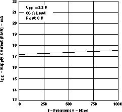
SN65HVD230 SN65HVD231 SN65HVD232 idd_f_los346.gif
Figure 1. Supply Current (RMS) vs Frequency
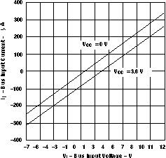
SN65HVD230 SN65HVD231 SN65HVD232 bicc_bvcc_los346.gif
Figure 3. Bus Input Current vs Bus Input Voltage
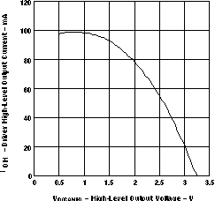
SN65HVD230 SN65HVD231 SN65HVD232 dioh_voh_los346.gif
Figure 5. Driver High-Level Output Current vs High-Level Output Voltage
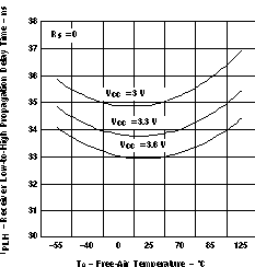
SN65HVD230 SN65HVD231 SN65HVD232 rlhtpd_ta_los346.gif
Figure 7. Receiver Low-to-High Propagation Delay Time vs Free-Air Temperature
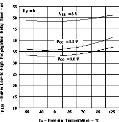
SN65HVD230 SN65HVD231 SN65HVD232 dlhtpd_ta_los346.gif
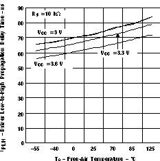
Figure 9. Driver Low-to-High Propagation Delay Time vs Free-Air Temperature
SN65HVD230 SN65HVD231 SN65HVD232 dlhtpd_ta2_los346.gif
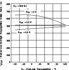
Figure 11. Driver Low-to-High Propagation Delay Time vs Free-Air Temperature
SN65HVD230 SN65HVD231 SN65HVD232 dlhtpd_ta3_los346.gif
Figure 13. Driver Low-to-High Propagation Delay Time vs Free-Air Temperature
SN65HVD230 SN65HVD231 SN65HVD232 dio_vdd_los346.gif
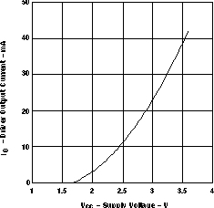
Figure 15. Driver Output Current vs Supply Voltage
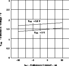
SN65HVD230 SN65HVD231 SN65HVD232 vref_iref_los346.gif
Figure 17. Reference Voltage vs Reference Current
SN65HVD230 SN65HVD231 SN65HVD232 licc_vdd_los346.gif
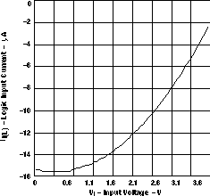
Figure 2. Logic Input Current (Pin D) vs Input Voltage
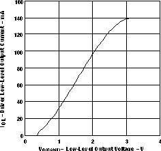
SN65HVD230 SN65HVD231 SN65HVD232 diol_vol_los346.gif
Figure 4. Driver Low-Level Output Current vs Low-Level Output Voltage
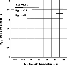
SN65HVD230 SN65HVD231 SN65HVD232 vod_ta_los346.gif
Figure 6. Dominant Voltage (VOD) vs Free-Air Temperature
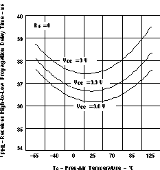
SN65HVD230 SN65HVD231 SN65HVD232 rhltpd_ta_los346.gif
Figure 8. Receiver High-to-Low Propagation Delay Time vs Free-Air Temperature
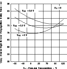
SN65HVD230 SN65HVD231 SN65HVD232 dhltpd_ta_los346.gif
Figure 10. Driver High-to-Low Propagation Delay Time vs Free-Air Temperature
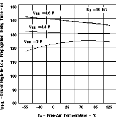
SN65HVD230 SN65HVD231 SN65HVD232 dhltpd_ta2_los346.gif
Figure 12. Driver High-to-Low Propagation Delay Time vs Free-Air Temperature
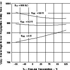
SN65HVD230 SN65HVD231 SN65HVD232 dhltpd_ta3_los346.gif
Figure 14. Driver High-to-Low Propagation Delay Time vs Free-Air Temperature
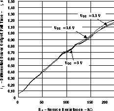
SN65HVD230 SN65HVD231 SN65HVD232 ddoft_los346.gif
Figure 16. Differential Driver Output Fall Time vs Source Resistance (Rs)