ZHCSDL3O MARCH   2001  – April 2018 SN65HVD230 , SN65HVD231 , SN65HVD232

PRODUCTION DATA.  

  1. 特性
  2. 应用
  3. 说明
    1.     Device Images
      1.      等效输入和输出原理图
  4. 修订历史记录
  5. 说明 (续)
  6. Device Comparison Table
  7. Pin Configuration and Functions
    1.     Pin Functions
  8. Specifications
    1. 8.1  Absolute Maximum Ratings
    2. 8.2  ESD Ratings
    3. 8.3  Recommended Operating Conditions
    4. 8.4  Thermal Information
    5. 8.5  Electrical Characteristics: Driver
    6. 8.6  Electrical Characteristics: Receiver
    7. 8.7  Switching Characteristics: Driver
    8. 8.8  Switching Characteristics: Receiver
    9. 8.9  Switching Characteristics: Device
    10. 8.10 Device Control-Pin Characteristics
    11. 8.11 Typical Characteristics
  9. Parameter Measurement Information
  10. 10Detailed Description
    1. 10.1 Overview
    2. 10.2 Functional Block Diagram
    3. 10.3 Feature Description
      1. 10.3.1 Vref Voltage Reference
      2. 10.3.2 Thermal Shutdown
    4. 10.4 Device Functional Modes
      1. 10.4.1 High-Speed Mode
      2. 10.4.2 Slope Control Mode
      3. 10.4.3 Standby Mode (Listen Only Mode) of the HVD230
      4. 10.4.4 The Babbling Idiot Protection of the HVD230
      5. 10.4.5 Sleep Mode of the HVD231
      6. 10.4.6 Summary of Device Operating Modes
  11. 11Application and Implementation
    1. 11.1 Application Information
      1. 11.1.1 CAN Bus States
    2. 11.2 Typical Application
      1. 11.2.1 Design Requirements
        1. 11.2.1.1 CAN Termination
        2. 11.2.1.2 Loop Propagation Delay
        3. 11.2.1.3 Bus Loading, Length and Number of Nodes
      2. 11.2.2 Detailed Design Procedure
        1. 11.2.2.1 Transient Protection
        2. 11.2.2.2 Transient Voltage Suppressors
      3. 11.2.3 Application Curve
    3. 11.3 System Example
      1. 11.3.1 ISO 11898 Compliance of SN65HVD23x Family of 3.3 V CAN Transceivers
        1. 11.3.1.1 Introduction
        2. 11.3.1.2 Differential Signal
          1. 11.3.1.2.1 Common Mode Signal
        3. 11.3.1.3 Interoperability of 3.3-V CAN in 5-V CAN Systems
  12. 12Power Supply Recommendations
  13. 13Layout
    1. 13.1 Layout Guidelines
    2. 13.2 Layout Example
  14. 14器件和文档支持
    1. 14.1 相关链接
    2. 14.2 接收文档更新通知
    3. 14.3 社区资源
    4. 14.4 商标
    5. 14.5 静电放电警告
    6. 14.6 Glossary
  15. 15机械、封装和可订购信息

封装选项

机械数据 (封装 | 引脚)
散热焊盘机械数据 (封装 | 引脚)
订购信息

Slope Control Mode

Electromagnetic compatibility is essential in many applications while still making use of unshielded twisted pair bus cable to reduce system cost. Slope control mode was added to the SN65HVD230 and SN65HVD231 devices to reduce the electromagnetic interference produced by the rise and fall times of the driver and resulting harmonics. These rise and fall slopes of the driver outputs can be adjusted by connecting a resistor from RS (pin 8) to ground or to a logic low voltage, as shown in Figure 32. The slope of the driver output signal is proportional to the pin's output current. This slope control is implemented with an external resistor value of 10 kΩ to achieve a ~15 V/μs slew rate, and up to 100 kΩ to achieve a ~2.0 V/μs slew rate as displayed in Figure 33.

SN65HVD230 SN65HVD231 SN65HVD232 ai_conn2_los346.gifFigure 32. Slope Control/Standby Connection to a DSP
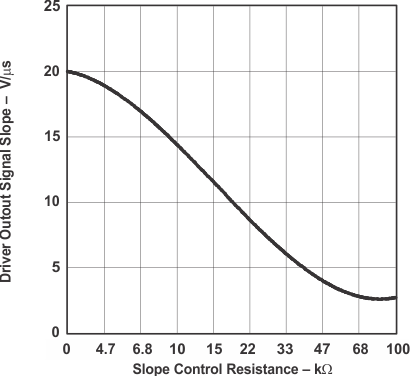
SN65HVD230 SN65HVD231 SN65HVD232 ai_slope1_los346.gifFigure 33. HVD230 Driver Output Signal Slope vs Slope Control Resistance Value