ZHCSDL3O MARCH 2001 – April 2018 SN65HVD230 , SN65HVD231 , SN65HVD232
PRODUCTION DATA.
- 1 特性
- 2 应用
- 3 说明
- 4 修订历史记录
- 5 说明 (续)
- 6 Device Comparison Table
- 7 Pin Configuration and Functions
-
8 Specifications
- 8.1 Absolute Maximum Ratings
- 8.2 ESD Ratings
- 8.3 Recommended Operating Conditions
- 8.4 Thermal Information
- 8.5 Electrical Characteristics: Driver
- 8.6 Electrical Characteristics: Receiver
- 8.7 Switching Characteristics: Driver
- 8.8 Switching Characteristics: Receiver
- 8.9 Switching Characteristics: Device
- 8.10 Device Control-Pin Characteristics
- 8.11 Typical Characteristics
- 9 Parameter Measurement Information
- 10Detailed Description
- 11Application and Implementation
- 12Power Supply Recommendations
- 13Layout
- 14器件和文档支持
- 15机械、封装和可订购信息
9 Parameter Measurement Information
 Figure 18. Driver Voltage and Current Definitions
 Figure 19. Driver VOD
 Figure 20. Driver Output Voltage Definitions
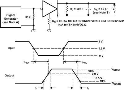
A. The input pulse is supplied by a generator having the following characteristics: PRR ≤ 500 kHz, 50% duty cycle, tr ≤ 6 ns, tf ≤ 6 ns, Zo = 50 Ω.
B. CL includes probe and jig capacitance.
Figure 21. Driver Test Circuit and Voltage Waveforms
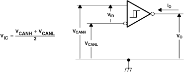 Figure 22. Receiver Voltage and Current Definitions

A. The input pulse is supplied by a generator having the following characteristics: PRR ≤ 500 kHz, 50% duty cycle, tr ≤ 6 ns, tf ≤ 6 ns, Zo = 50 Ω.
B. CL includes probe and jig capacitance.
Figure 23. Receiver Test Circuit and Voltage Waveforms
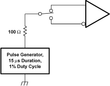 Figure 24. Overvoltage Protection
Table 1. Receiver Characteristics Over Common Mode With V(Rs) = 1.2 V
| VIC | VID | VCANH | VCANL | R OUTPUT | |
|---|---|---|---|---|---|
| -2 V | 900 mV | -1.55 V | -2.45 V | L | VOL |
| 7 V | 900 mV | 8.45 V | 6.55 V | L | |
| 1 V | 6 V | 4 V | -2 V | L | |
| 4 V | 6 V | 7 V | 1 V | L | |
| -2 V | 500 mV | -1.75 V | -2.25 V | H | VOH |
| 7 V | 500 mV | 7.25 V | 6.75 V | H | |
| 1 V | -6 V | -2 V | 4 V | H | |
| 4 V | -6 V | 1 V | 7 V | H | |
| X | X | Open | Open | H | |
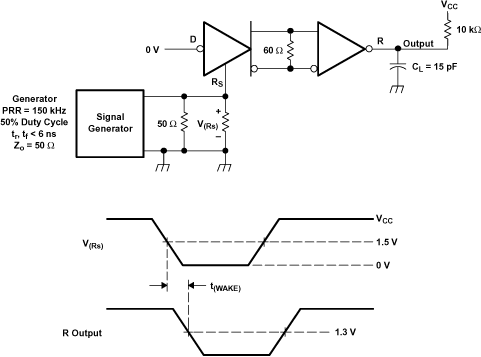 Figure 25. t(WAKE) Test Circuit and Voltage Waveforms
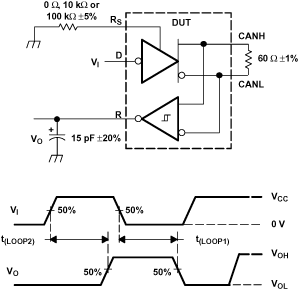
A. All VI input pulses are supplied by a generator having the following characteristics: tr or tf ≤ 6 ns, Pulse Repetition Rate (PRR) = 125 kHz, 50% duty cycle.
Figure 26. t(LOOP) Test Circuit and Voltage Waveforms
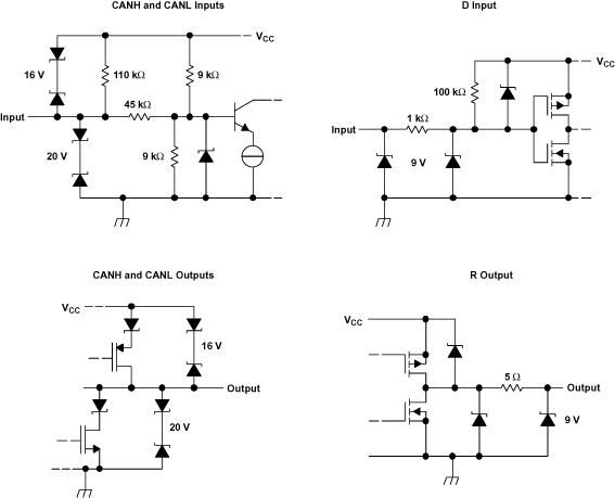 Figure 27. Equivalent Input and Output Schematic Diagrams