ZHCSDL3O MARCH 2001 – April 2018 SN65HVD230 , SN65HVD231 , SN65HVD232
PRODUCTION DATA.
- 1 特性
- 2 应用
- 3 说明
- 4 修订历史记录
- 5 说明 (续)
- 6 Device Comparison Table
- 7 Pin Configuration and Functions
-
8 Specifications
- 8.1 Absolute Maximum Ratings
- 8.2 ESD Ratings
- 8.3 Recommended Operating Conditions
- 8.4 Thermal Information
- 8.5 Electrical Characteristics: Driver
- 8.6 Electrical Characteristics: Receiver
- 8.7 Switching Characteristics: Driver
- 8.8 Switching Characteristics: Receiver
- 8.9 Switching Characteristics: Device
- 8.10 Device Control-Pin Characteristics
- 8.11 Typical Characteristics
- 9 Parameter Measurement Information
- 10Detailed Description
- 11Application and Implementation
- 12Power Supply Recommendations
- 13Layout
- 14器件和文档支持
- 15机械、封装和可订购信息
11.3.1.3 Interoperability of 3.3-V CAN in 5-V CAN Systems
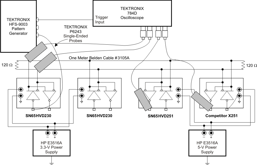
The 3.3 V supplied SN65HVD23x family of CAN transceivers are fully compatible with 5 V CAN transceivers. The differential output voltage is the same, the recessive common mode output bias is the same, and the receivers have the same input specifications. The only difference is in the dominant common mode output voltage is lower in 3.3 V CAN transceivers than with 5 V supplied transceiver (by a few hundred millivolts).
To help ensure the widest interoperability possible, the SN65HVD23x family has successfully passed the internationally recognized GIFT ICT conformance and interoperability testing for CAN transceivers which is shown in . Electrical interoperability does not always assure interchangeability however. Most implementers of CAN buses recognize that ISO 11898 does not sufficiently specify the electrical layer and that strict standard compliance alone does not ensure full interchangeability. This comes only with thorough equipment testing.
