SLLS933G November 2008 – January 2015 SN65HVD233-HT
PRODUCTION DATA.
- 1 Features
- 2 Applications
- 3 Description
- 4 Revision History
- 5 Description (Continued)
- 6 Pin Configuration and Functions
-
7 Specifications
- 7.1 Absolute Maximum Ratings
- 7.2 ESD Ratings
- 7.3 Recommended Operating Conditions
- 7.4 Thermal Information
- 7.5 Driver Electrical Characteristics
- 7.6 Receiver Electrical Characteristics
- 7.7 Driver Switching Characteristics
- 7.8 Receiver Switching Characteristics
- 7.9 Device Switching Characteristics
- 7.10 Typical Characteristics
- 8 Parameter Measurement Information
- 9 Detailed Description
- 10Application and Implementation
- 11Power Supply Recommendations
- 12Layout
- 13Device and Documentation Support
- 14Mechanical, Packaging, and Orderable Information
封装选项
机械数据 (封装 | 引脚)
散热焊盘机械数据 (封装 | 引脚)
订购信息
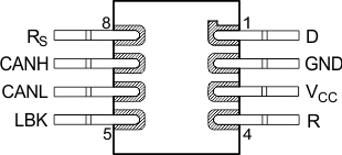
6 Pin Configuration and Functions
D, JDJ, and HKJ Packages
8-Pin SOIC, CDIP SB, and CFP
Top View

HKQ Package
8-Pin CFP
Top View

HKQ as formed or HKJ mounted dead bug.
Pin Functions
| PIN | TYPE | DESCRIPTION | |
|---|---|---|---|
| NO. | NAME | ||
| 1 | D | I | CAN Transmit Data input (Low for dominant and HIGH for recessive bus states) |
| 2 | GND | Power | Ground connection |
| 3 | VCC | Power | VCC |
| 4 | R | O | CAN Receive data output |
| 5 | LBK | I | LoopBack (Active high to enable controller loopback mode) |
| 6 | CFANL | I/O | Low level CAN bus line |
| 7 | CANH | I/O | High level CAN bus line |
| 8 | Rs | I | High Speed, Slope control, and standby enable mode input. |
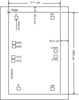
Bare Die Information
| DIE THICKNESS | BACKSIDE FINISH | BACKSIDE POTENTIAL | BOND PAD METALLIZATION COMPOSITION |
|---|---|---|---|
| 15 mils. | Silicon with backgrind | GND | Al-Si-Cu (0.5%) |

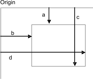
Bond Pad Coordinates In Microns - Rev A
| DESCRIPTION | PAD NUMBER | A | B | C | D |
|---|---|---|---|---|---|
| D | 1 | 86.40 | 157.85 | 203.40 | 274.85 |
| GND | 2 | 1035.05 | 69.75 | 1150.05 | 184.75 |
| GND | 3 | 1168.15 | 69.75 | 1283.15 | 184.75 |
| VCC | 4 | 1572.05 | 51.85 | 1687.05 | 166.85 |
| VCC | 5 | 1711.95 | 51.85 | 1826.95 | 166.85 |
| R | 6 | 2758.85 | 237.65 | 2873.85 | 352.65 |
| LBK | 7 | 2774.25 | 1429.985 | 2889.25 | 1544.95 |
| CANL | 8 | 1549.90 | 1544.95 | 1664.90 | 1659.95 |
| CANH | 9 | 1351.45 | 1544.95 | 1466.45 | 1659.95 |
| RS | 10 | 83.50 | 1429.95 | 198.50 | 1544.95 |
