SLLS545G November 2002 – October 2015 SN55HVD251 , SN65HVD251
PRODUCTION DATA.
- 1 Features
- 2 Applications
- 3 Description
- 4 Revision History
- 5 Pin Configuration and Functions
-
6 Specifications
- 6.1 Absolute Maximum Ratings
- 6.2 ESD Ratings
- 6.3 Recommended Operating Conditions
- 6.4 Thermal Information
- 6.5 Supply Current
- 6.6 Electrical Characteristics: Driver
- 6.7 Electrical Characteristics: Receiver
- 6.8 VREF-Pin Characteristics
- 6.9 Power Dissipation Characteristics
- 6.10 Switching Characteristics: Driver
- 6.11 Switching Characteristics: Device
- 6.12 Switching Characteristics: Receiver
- 6.13 Dissipation Ratings
- 6.14 Typical Characteristics
- 7 Parameter Measurement Information
- 8 Detailed Description
- 9 Application and Implementation
- 10Power Supply Recommendations
- 11Layout
- 12Device and Documentation Support
- 13Mechanical, Packaging, and Orderable Information
9 Application and Implementation
NOTE
Information in the following applications sections is not part of the TI component specification, and TI does not warrant its accuracy or completeness. TI’s customers are responsible for determining suitability of components for their purposes. Customers should validate and test their design implementation to confirm system functionality.
9.1 Application Information
The CAN bus has two states during powered operation of the device; dominant and recessive. A dominant bus state is when the bus is driven differentially, corresponding to a logic low on the D and R pin. A recessive bus state is when the bus is biased to VCC/2 via the high-resistance internal resistors RIN and RID of the receiver, corresponding to a logic high on the D and R pins. See Figure 26 and Figure 27.
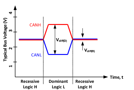 Figure 26. Bus States
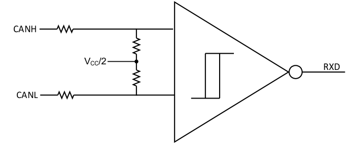 Figure 27. Simplified Recessive Common Mode Bias and Receiver
The HVD251 CAN transceiver is typically used in applications with a host microprocessor or FPGA that includes the link layer portion of the CAN protocol. The different nodes on the network are typically connected through the use of a 120-Ω characteristic impedance twisted pair cable with termination on both ends of the bus.
The basics of bus arbitration require that the receiver at the sending node designate the first bit as dominant or recessive after the initial wave of the first bit of a message travels to the most remote node on a network and back again. Typically, this sample is made at 75% of the bit width, and within this limitation, the maximum allowable signal distortion in a CAN network is determined by network electrical parameters.
Factors to be considered in network design include the 5 ns/m propagation delay of typical twisted-pair bus cable; signal amplitude loss due to the loss mechanisms of the cable; and the number, length, and spacing of drop-lines (stubs) on a network. Under strict analysis, variations among the different oscillators in a system must also be accounted for with adjustments in signaling rate and stub and bus length. Table 4 lists the maximum signaling rates achieved with the HVD251 in high-speed mode with several bus lengths of category-5, shielded twisted-pair (CAT 5 STP) cable.
Table 4. Maximum Signaling Rates for Various Cable Lengths
| BUS LENGTH (m) | SIGNALING RATE (kbps) |
|---|---|
| 30 | 1000 |
| 100 | 500 |
| 250 | 250 |
| 500 | 125 |
| 1000 | 62.5 |
The ISO 11898 standard specifies a maximum bus length of 40 meters and maximum stub length of 0.3 meters with a maximum of 30 nodes. However, with careful design, users can have longer cables, longer stub lengths, and many more nodes on a bus. (Note: Non-standard application may come with a trade-off in signaling rate.) A bus with a large number of nodes requires a transceiver with high input impedance such as the HVD251.
The Standard specifies the interconnect to be a single twisted-pair cable (shielded or unshielded) with 120-Ω characteristic impedance (Zo). Resistors equal to the characteristic impedance of the line terminate both ends of the cable to prevent signal reflections. Unterminated drop-lines connect nodes to the bus and should be kept as short as possible to minimize signal reflections.
Connectors, while not specified by the ISO 11898 standard, should have as little effect as possible on standard operating parameters such as capacitive loading. Although unshielded cable is used in many applications, data transmission circuits employing CAN transceivers are usually used in applications requiring a rugged interconnection with a wide common-mode voltage range. Therefore, shielded cable is recommended in these electronically harsh environments, and when coupled with the –2-V to 7-V common-mode range of tolerable ground noise specified in the standard, helps to ensure data integrity. The HVD251 extends data integrity beyond that of the standard with an extended –7-V to 12-V range of common-mode operation.
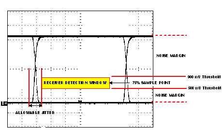 Figure 28. Typical CAN Differential Signal Eye-Pattern
An eye pattern is a useful tool for measuring overall signal quality. As displayed in Figure 28, the differential signal changes logic states in two places on the display, producing an eye. Instead of viewing only one logic crossing on the scope, an entire bit of data is brought into view. The resulting eye pattern includes all effects of systemic and random distortion, and displays the time during which a signal may be considered valid.
The height of the eye above or below the receiver threshold voltage level at the sampling point is the noise margin of the system. Jitter is typically measured at the differential voltage zero-crossing during the logic state transition of a signal. Note that jitter present at the receiver threshold voltage level is considered by some to be a more effective representation of the jitter at the input of a receiver.
As the sum of skew and noise increases, the eye closes and data is corrupted. Closing the width decreases the time available for accurate sampling, and lowering the height enters the 900-mV or 500-mV threshold of a receiver.
Different sources induce noise onto a signal. The more obvious noise sources are the components of a transmission circuit themselves; the signal transmitter, traces & cables, connectors, and the receiver. Beyond that, there is a termination dependency, cross-talk from clock traces and other proximity effects, VCC and ground bounce, and electromagnetic interference from near-by electrical equipment.
The balanced receiver inputs of the HVD251 mitigate most sources of signal corruption, and when used with a quality shielded twisted-pair cable, help meet data integrity.
9.2 Typical Application
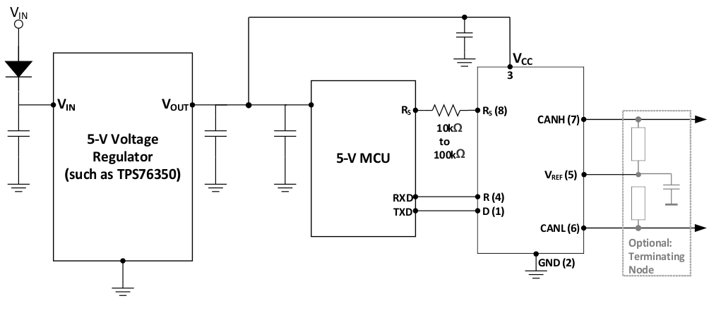 Figure 29. Typical Application Schematic
9.2.1 Design Requirements
9.2.1.1 Bus Loading, Length, and Number of Nodes
The ISO11898 Standard specifies up to 1-Mbps data rate, maximum bus length of 40 meters, maximum drop line (stub) length of 0.3 meters and a maximum of 30 nodes. However, with careful network design, the system may have longer cables, longer stub lengths, and many more nodes to a bus. Many CAN organizations and standards have scaled the use of CAN for applications outside the original ISO11898 standard. They have made system level trade-offs for data rate, cable length, and parasitic loading of the bus. Examples of some of these specifications are ARINC825, CANopen, CAN Kingdom, DeviceNet and NMEA200.
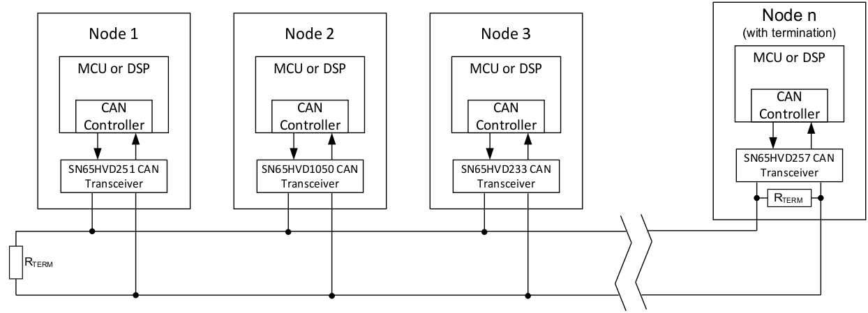 Figure 30. Typical CAN Bus
A high number of nodes requires a transceiver with high input impedance and wide common mode range such as the SNx5HVD251 CAN transceiver. ISO11898-2 specifies the driver differential output with a 60-Ω load (two 120-Ω termination resistors in parallel) and the differential output must be greater than 1.5 V. The SNx5HVD251 devices are specified to meet the 1.5-V requirement with a 60-Ω load, and additionally specified with a differential output voltage minimum of 1.2 V across a common mode range of –2 V to 7 V via a 330-Ω coupling network. This network represents the bus loading of 120 SNx5HVD251 transceivers based on their minimum differential input resistance of 40 kΩ. Therefore, the SNx5HVD251 supports up to 120 transceivers on a single bus segment with margin to the 1.2-V minimum differential input voltage requirement at each node.
For CAN network design, margin must be given for signal loss across the system and cabling, parasitic loadings, network imbalances, ground offsets and signal integrity thus a practical maximum number of nodes may be lower. Bus length may also be extended beyond the original ISO 11898 standard of 40 meters by careful system design and data rate tradeoffs. For example, CANopen network design guidelines allow the network to be up to 1 km with changes in the termination resistance, cabling, less than 64 nodes and significantly lowered data rate.
This flexibility in CAN network design is one of the key strengths of the various extensions and additional standards that have been built on the original ISO 11898 CAN standard.
9.2.2 Detailed Design Procedure
9.2.2.1 CAN Termination
The ISO 11898 standard specifies the interconnect to be a twisted pair cable (shielded or unshielded) with 120-Ω characteristic impedance (ZO ). Resistors equal to the characteristic impedance of the line should be used to terminate both ends of the cable to prevent signal reflections. Unterminated drop lines (stubs) connecting nodes to the bus should be kept as short as possible to minimize signal reflections. The termination may be on the cable or in a node, but if nodes may be removed from the bus the termination must be carefully placed so that it is not removed from the bus.
Termination is typically a 120-Ω resistor at each end of the bus. If filtering and stabilization of the common mode voltage of the bus is desired, then split termination may be used (see Figure 30). Split termination utilizes two 60- Ω resistors with a capacitor in the middle of these resistors to ground. Split termination improves the electromagnetic emissions behavior of the network by eliminating fluctuations in the bus common mode voltages at the start and end of message transmissions.
Care should be taken when determining the power ratings of the termination resistors. A typical worst case fault condition is if the system power supply and ground were shorted across the termination resistance which would result in much higher current through the termination resistance than the CAN transceiver's current limit.
 Figure 31. CAN Termination
9.2.2.2 Loop Propagation Delay
Transceiver loop delay is a measure of the overall device propagation delay, consisting of the delay from the driver input (D pin) to the differential outputs (CANH and CANL pins), plus the delay from the receiver inputs (CANH and CANL) to its output pin.
A typical loop delay for the SNx5HVD251 transceiver is displayed in Figure 32. This loop delay will increase as the slope of the driver output is slowed during slope control mode. This increased loop delay means that there is a tradeoff between the total bus length able to be used and the driver's output slope used via the slope control pin of the device. For example, the loop delay for a 10-kΩ resistor from the RS pin to ground is ~100 ns, and the loop delay for a 100-kΩ resistor is ~500 ns. Therefore, if we use the following rule-of-thumb that the propagation delay of typical twisted pair bus cable is 5 ns/m, we can calculate an approximate cable length trade-off between normal high-speed mode and slope control mode with a 100-kΩ resistor. Using typical values, the loop delay for a recessive to dominant bit with RS tied directly to ground is 60ns, and with a 100-kΩ resistor is 440 ns. At 5-ns/m of propagation delay, which you have to count in both directions the difference is 38 meters (440 – 60)/(2 × 5).
Another option to improving the electromagnetic emissions of the device besides slowing down the edge rates of the driver in slope control mode is using quality shielded bus cabling.
9.2.3 Application Curve
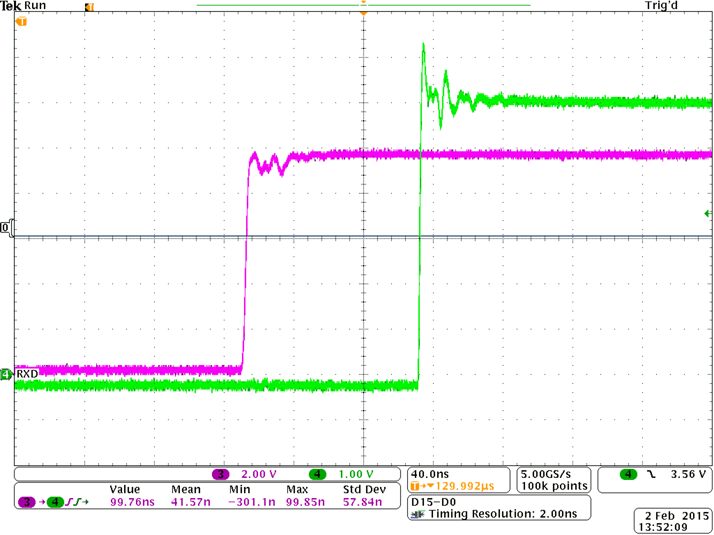 Figure 32. tLOOP Delay
9.3 System Example
9.3.1 ISO 11898 Compliance of HVD251 5-V CAN Bus Transceiver
9.3.1.1 Introduction
The SNx5HVD251 CAN transceiver is a 5-V CAN transceiver that meets or exceeds the specification of the ISO 11898 standard for applications employing a controller area network.
9.3.1.2 Differential Signal
CAN is a differential bus where complementary signals are sent over two wires and the voltage difference between the two wires defines the logical state of the bus. The differential CAN receiver monitors this voltage difference and outputs the bus state with a single ended logic level output signal.
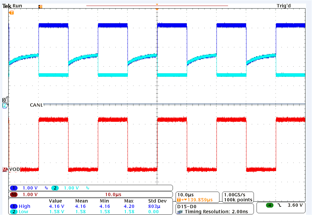 Figure 33. Differential Output Waveform
The CAN driver creates the differential voltage between CANH and CANL in the dominant state. The dominant differential output of the HVD251 is greater than 1.5 V and less than 3 V across a 60-Ω load as defined by the ISO 11898 standard. Figure 33 shows CANH, CANL, and the differential dominant state level for the SNx5HVD251.
A CAN receiver is required to output a recessive state when less than 500 mV of differential voltage exists on the bus, and a dominant state when more than 900 mV of differential voltage exists on the bus. The CAN receiver must do this with common-mode input voltages from –2 V to 7 V.
9.3.1.3 Common-Mode Signal
A common-mode signal is an average voltage of the two signal wires that the differential receiver rejects. The common-mode signal comes from the CAN driver, ground noise, and coupled bus noise. Since the bias voltage of the recessive state of the device is dependent on VCC, any noise present or variation of VCC will have an effect on this bias voltage seen by the bus. The HVD251 CAN transceiver has the recessive bias voltage set to 0.5 × VCC to comply with the ISO 11898-2 CAN standard.