ZHCSBN6A September 2013 – November 2015 SN65HVD265 , SN65HVD266 , SN65HVD267
PRODUCTION DATA.
- 1 特性
- 2 应用
- 3 (说明
- 4 Revision History
- 5 Device Comparison Table
- 6 Pin Configurations and Functions
- 7 Specifications
- 8 Parameter Measurement Information
- 9 Detailed Description
- 10Application and Implementation
- 11Power Supply Recommendations
- 12Layout
- 13器件和文档支持
- 14机械、封装和可订购信息
12 Layout
12.1 Layout Guidelines
For the PCB design to be successful, start with design of the protection and filtering circuitry. Because ESD and EFT transients have a wide frequency bandwidth from approximately 3 MHz to 3 GHz, high frequency layout techniques must be applied during PCB design. On chip IEC ESD protection is good for laboratory and portable equipment but is usually not sufficient for EFT and surge transients occurring in industrial environments. Therefore, robust and reliable bus node design requires the use of external transient protection devices at the bus connectors. Placement at the connector also prevents these noisy events from propagating further into the PCB and system.
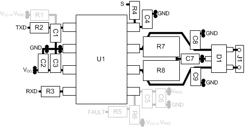
- Place the protection and filtering circuitry as close to the bus connector, J1, to prevent transients, ESD and noise from penetrating onto the board. In this layout example for protection a Transient Voltage Suppression (TVS) device, D1, has been used. The production solution can be either bi-directional TVS diode or varistor with ratings matching the application requirements. This example also shows optional bus filter capacitors C8 and C9.
- Design the bus protection components in the direction of the signal path. Do not force the transient current to divert from the signal path to reach the protection device.
- Use supply (VCC) and ground planes to provide low inductance. Note: high frequency current follows the path of least inductance and not the path of least impedance.
- Use at least two vias for supply (VCC) and ground connections of bypass capacitors and protection devices to minimize trace and via inductance.
- Bypass and bulk capacitors should be placed as close as possible to the supply terminals of transceiver, examples C2, C3 (VCC) and for the dual supply devices additionally C5 and C6 (VRXD).
- Bus termination: this layout example shows split termination. This is where the termination is split into two resistors, R7 and R8, with the center or split tap of the termination connected to ground via capacitor C7. Split termination provides common mode filtering for the bus. When bus termination is placed on the board instead of directly on the bus, additional care must be taken to ensure the terminating node is not removed from the bus thus also removing the termination. See the application section for information on power ratings needed for the termination resistor(s).
- To limit current of digital lines serial resistors may be used. Examples are R2, R3, R4 and R5.
- To filter noise on the digital IO lines a capacitor may be used close to the input side of the IO as shown by C1 and C4.
- Terminal 5: This example is showing a flexible layout covering all three of the devices in this CAN transceiver family on terminal 5. SN65HVD265: this terminal is a no connect so external connections are un-important and the components R4, R5, C5 and C6 do not matter. SN65HVD266: this terminal is the RXD output supply terminal, VRXD. The bypass and bulk capacitor pads of C5 and C6 should be populated and R5 and R6 are not used. SN65HVD267: this terminal is the FAULT output (open drain). The pull resistor R6 is needed. R5 is shown if current limiting is desired to the host processor. If noise filtering is desired C5 should be used.
- 1k to 10kΩ pull-up or down resistors should be used where required to limit noise during transient events.
- Terminal 1: R1 is shown optionally for the TXD input of the device. If an option drain host processor is used this is mandatory to ensure the bit timing into the device is met.
- Terminal 8: is shown assuming the mode terminal, S, will be used. If the device will only be used in normal mode R3 is not needed and the pads of C4 could be used for the pull down resistor to GND.
12.2 Layout Example
 Figure 21. Layout Example