SGLS367E September 2006 – September 2015 SN65HVD30-EP , SN65HVD33-EP
PRODUCTION DATA.
- 1 Features
- 2 Applications
- 3 Description
- 4 Revision History
- 5 Pin Configuration and Functions
-
6 Specifications
- 6.1 Absolute Maximum Ratings
- 6.2 ESD Ratings
- 6.3 Recommended Operating Conditions
- 6.4 Thermal Information
- 6.5 Electrical Characteristics: Driver
- 6.6 Electrical Characteristics: Receiver
- 6.7 Switching Characteristics: Driver
- 6.8 Switching Characteristics: Receiver
- 6.9 Receiver Equalization Characteristics
- 6.10 Dissipation Ratings
- 6.11 Typical Characteristics
- 7 Parameter Measurement Information
- 8 Detailed Description
- 9 Application and Implementation
- 10Power Supply Recommendations
- 11Layout
- 12Device and Documentation Support
- 13Mechanical, Packaging, and Orderable Information
1 Features
- 1/8 Unit-Load Option Available (up to 256 Nodes on the Bus)
- Bus-Pin ESD Protection Exceeds 15 kV HBM
- Optional Driver Output Transition Times for Signaling Rates (1) of 1 Mbps, 5 Mbps, and 25 Mbps
- Low-Current Standby Mode: <1 μA
- Glitch-Free Power-Up and Power-Down Protection for Hot-Plugging Applications
- 5-V Tolerant Inputs
- Bus Idle, Open, and Short-Circuit Fail Safe
- Driver Current Limiting and Thermal Shutdown
- Meet or Exceed the Requirements of ANSI TIA/EIA-485-A and RS-422 Compatible
2 Applications
- Utility Meters
- DTE and DCE Interfaces
- Industrial, Process, and Building Automation
- Point-of-Sale (POS) Terminals and Networks
- Controlled Baseline
- One Assembly and Test Site
- One Fabrication Site
- Available in Military (–55°C/125°C) Temperature Range
- Extended Product Life Cycle
- Extended Product-Change Notification
- Product Traceability
3 Description
The SN65HVD3x-EP devices are 3-state differential line drivers and differential-input line receivers that operate with 3-V power supply.
Each driver and receiver has separate input and output pins for full-duplex bus communication designs. They are designed for balanced transmission lines and interoperation with ANSI TIA/EIA-485A, TIA/EIA-422-B, ITU-T v.11, and ISO 8482:1993 standard-compliant devices.
The SN65HVD30, SN65HVD31, and SN65HVD32 are fully enabled with no external enabling pins.
The SN65HVD33, SN65HVD34, and SN65HVD35 have active-high driver enables and active-low receiver enables. A low (less than 1 μA) standby current can be achieved by disabling both the driver and receiver.
All devices are characterized for operation from –55°C to 125°C.
Device Information(1)
| PART NUMBER | PACKAGE | BODY SIZE (NOM) |
|---|---|---|
| SN65HVD3x-EP | SOIC (8) | 4.90 mm x 3.91 mm |
| SOIC (14) | 8.65 mm x 3.91 mm |
- For all available packages, see the orderable addendum at the end of the datasheet.
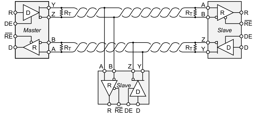
Typical Application Schematic
