SGLS367E September 2006 – September 2015 SN65HVD30-EP , SN65HVD33-EP
PRODUCTION DATA.
- 1 Features
- 2 Applications
- 3 Description
- 4 Revision History
- 5 Pin Configuration and Functions
-
6 Specifications
- 6.1 Absolute Maximum Ratings
- 6.2 ESD Ratings
- 6.3 Recommended Operating Conditions
- 6.4 Thermal Information
- 6.5 Electrical Characteristics: Driver
- 6.6 Electrical Characteristics: Receiver
- 6.7 Switching Characteristics: Driver
- 6.8 Switching Characteristics: Receiver
- 6.9 Receiver Equalization Characteristics
- 6.10 Dissipation Ratings
- 6.11 Typical Characteristics
- 7 Parameter Measurement Information
- 8 Detailed Description
- 9 Application and Implementation
- 10Power Supply Recommendations
- 11Layout
- 12Device and Documentation Support
- 13Mechanical, Packaging, and Orderable Information
7 Parameter Measurement Information
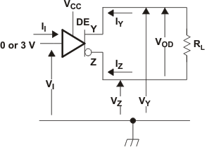
 Figure 10. Driver VOD Test Circuit and Voltage and Current Definitions
 Figure 11. Driver VOD With Common-Mode Loading Test Circuit
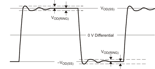
 Figure 12. VOD(RING) Waveform and Definitions
VOD(RING) is measured at four points on the output waveform, corresponding to overshoot and undershoot from the VOD(H) and VOD(L) steady state values.

Input: PRR = 500 kHz, 50% Duty Cycle, tr < 6 ns, tf < 6 ns, ZO = 50 Ω
Figure 13. Test Circuit and Definitions for Driver Common-Mode Output Voltage

A. Generator: PRR = 500 kHz, 50% Duty Cycle, tr < 6 ns, tf < 6 ns, ZO = 50 Ω
Figure 14. Driver Switching Test Circuit and Voltage Waveforms

A. Generator: PRR = 500 kHz, 50% Duty Cycle, tr < 6 ns, tf < 6 ns, ZO = 50 Ω
B. CL Includes Fixture and Instrumentation Capacitance
Figure 15. Driver High-Level Output Enable and Disable Time Test Circuit and Voltage Waveforms

A. Generator: PRR = 500 kHz, 50% Duty Cycle, tr < 6 ns, tf < 6 ns, ZO = 50 Ω
Figure 16. Driver Low-Level Output Enable and Disable Time Test Circuit and Voltage Waveforms
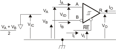
 Figure 17. Receiver Voltage and Current Definitions

A. CL Includes Fixture and Instrumentation Capacitance
B. Generator: PRR = 500 kHz, 50% Duty Cycle, tr < 6 ns, tf < 6 ns, ZO = 50 Ω
Figure 18. Receiver Switching Test Circuit and Voltage Waveforms

A. Generator: PRR = 500 kHz, 50% Duty Cycle, tr < 6 ns, tf < 6 ns, ZO = 50 Ω
Figure 19. Receiver High-Level Enable and Disable Time Test Circuit and Voltage Waveforms

A. Generator: PRR = 500 kHz, 50% Duty Cycle, tr < 6 ns, tf < 6 ns, ZO = 50 Ω
Figure 20. Receiver Enable Time From Standby (Driver Disabled)
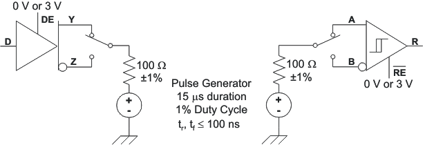
 Figure 21. Test Circuit, Transient Over Voltage Test