SGLS367E September 2006 – September 2015 SN65HVD30-EP , SN65HVD33-EP
PRODUCTION DATA.
- 1 Features
- 2 Applications
- 3 Description
- 4 Revision History
- 5 Pin Configuration and Functions
-
6 Specifications
- 6.1 Absolute Maximum Ratings
- 6.2 ESD Ratings
- 6.3 Recommended Operating Conditions
- 6.4 Thermal Information
- 6.5 Electrical Characteristics: Driver
- 6.6 Electrical Characteristics: Receiver
- 6.7 Switching Characteristics: Driver
- 6.8 Switching Characteristics: Receiver
- 6.9 Receiver Equalization Characteristics
- 6.10 Dissipation Ratings
- 6.11 Typical Characteristics
- 7 Parameter Measurement Information
- 8 Detailed Description
- 9 Application and Implementation
- 10Power Supply Recommendations
- 11Layout
- 12Device and Documentation Support
- 13Mechanical, Packaging, and Orderable Information
9 Application and Implementation
NOTE
Information in the following applications sections is not part of the TI component specification, and TI does not warrant its accuracy or completeness. TI’s customers are responsible for determining suitability of components for their purposes. Customers should validate and test their design implementation to confirm system functionality.
9.1 Application Information
The SN65HVD3x-EP family consists of full-duplex RS-485 transceivers commonly used for asynchronous data transmissions. Full-duplex implementation requires two signal pairs (four wires), and allows each node to transmit data on one pair while simultaneously receiving data on the other pair.
To eliminate line reflections, each cable end is terminated with a termination resistor (RT) whose value matches the characteristic impedance (Z0) of the cable. This method, known as parallel termination, allows for higher data rates over longer cable length.
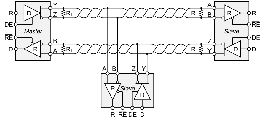 Figure 27. Typical RS-485 Network With Full-Duplex Transceivers
9.2 Typical Application
A full-duplex RS-485 network consists of multiple transceivers connecting in parallel to two bus cables. On one signal pair, a master driver transmits data to multiple slave receivers. The master driver and slave receivers can remain fully enabled at all times. On the other signal pair, multiple slave drivers transmit data to the master receiver. To avoid bus contention, the slave drivers must be intermittently enabled and disabled such that only one driver is enabled at any time, as in half-duplex communication. The master receiver can remain fully enabled at all times.
Because the driver cannot be disabled, only connect one driver to the bus when using the SN65HVD30, SN65HVD31, or SN65HVD32 devices.
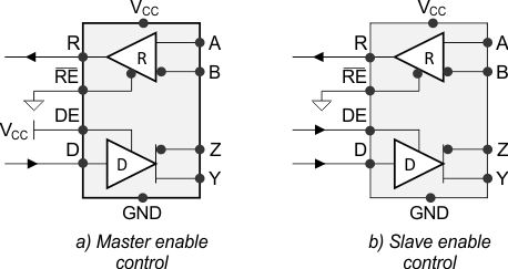 Figure 28. Full-Duplex Transceiver Configurations
9.2.1 Design Requirements
RS-485 is a robust electrical standard suitable for long-distance networking that may be used in a wide range of applications with varying requirements, such as distance, data rate, and number of nodes.
9.2.1.1 Data Rate and Bus Length
There is an inverse relationship between data rate and bus length, meaning the higher the data rate, the shorter the cable length; and conversely, the lower the data rate, the longer the cable can be without introducing data errors. While most RS-485 systems use data rates between 10 kbps and 100 kbps, some applications require data rates up to 250 kbps at distances of 4000 feet and longer. Longer distances are possible by allowing for small signal jitter of up to 5 or 10%.
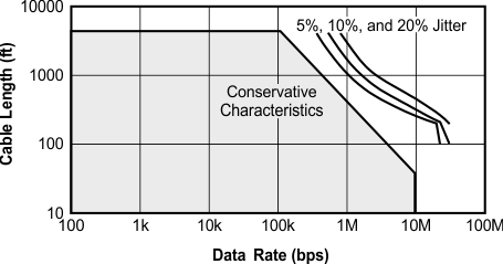 Figure 29. Cable Length vs Data Rate Characteristic
Even higher data rates are achievable (such as 26 Mbps for the SN65HVD30 and SN65HVD33 devices) in cases where the interconnect is short enough (or has suitably low attenuation at signal frequencies) to not degrade the data.
9.2.1.2 Stub Length
When connecting a node to the bus, the distance between the transceiver inputs and the cable trunk, known as the stub, must be as short as possible. Stubs present a nonterminated piece of bus line that can introduce reflections as the length of the stub increases. As a general guideline, the electrical length, or round-trip delay, of a stub must be less than one-tenth of the rise time of the driver; thus giving a maximum physical stub length as shown in Equation 1.
where
- tr is the 10/90 rise time of the driver
- c is the speed of light (3 × 10⁸ m/s)
- v is the signal velocity of the cable or trace as a factor of c
Per Equation 1, Table 8 shows the maximum cable-stub lengths for the minimum driver output rise times of the SN65HVD3x-EP full-duplex family of transceivers for a signal velocity of 78%.
Table 8. Maximum Stub Length
| DEVICE | MINIMUM DRIVER OUTPUT RISE TIME (ns) | MAXIMUM STUB LENGTH | |
|---|---|---|---|
| (m) | (ft) | ||
| SN65HVD30 | 4 | 0.1 | 0.3 |
| SN65HVD31 | 25 | 0.6 | 1.9 |
| SN65HVD32 | 120 | 2.8 | 9.2 |
| SN65HVD33 | 4 | 0.1 | 0.3 |
| SN65HVD34 | 25 | 0.6 | 1.9 |
| SN65HVD35 | 120 | 2.8 | 9.2 |
9.2.1.3 Bus Loading
The RS-485 standard specifies that a compliant driver must be able to driver 32 unit loads (UL), where 1 unit load represents a load impedance of approximately 12 kΩ. Because the SN65HVD30 and SN65HVD33 devices are 1/2 UL transceivers, it is possible to connect up to 64 receivers to the bus. Likewise, the SN65HVD31, SN65HVD32, SN65HVD34, and SN65HVD35 devices are 1/8 UL transceivers that can support up to 256 receivers.
9.2.2 Detailed Design Procedure
To protect bus nodes against high-energy transients, the implementation of external transient protection devices is necessary (see Figure 30).
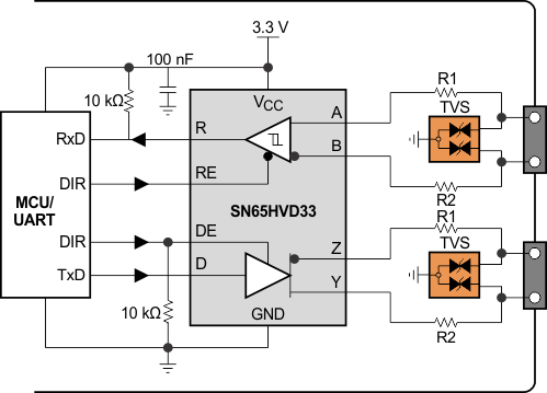 Figure 30. Transient Protection Against ESD, EFT, and Surge Transients
Table 9. Bill of Materials
| DEVICE | FUNCTION | ORDER NUMBER | MANUFACTURER |
|---|---|---|---|
| XCVR | 3.3-V Full-Duplex RS-485 Transceiver | SN65HVD33 | TI |
| R1, R2 | 10-Ω, Pulse-Proof Thick-Film Resistor | CRCW060310RJNEAHP | Vishay |
| TVS | Bidirectional 400-W Transient Suppressor | CDSOT23-SM712 | Bourns |
9.2.3 Application Curve
