SGLS367E September 2006 – September 2015 SN65HVD30-EP , SN65HVD33-EP
PRODUCTION DATA.
- 1 Features
- 2 Applications
- 3 Description
- 4 Revision History
- 5 Pin Configuration and Functions
-
6 Specifications
- 6.1 Absolute Maximum Ratings
- 6.2 ESD Ratings
- 6.3 Recommended Operating Conditions
- 6.4 Thermal Information
- 6.5 Electrical Characteristics: Driver
- 6.6 Electrical Characteristics: Receiver
- 6.7 Switching Characteristics: Driver
- 6.8 Switching Characteristics: Receiver
- 6.9 Receiver Equalization Characteristics
- 6.10 Dissipation Ratings
- 6.11 Typical Characteristics
- 7 Parameter Measurement Information
- 8 Detailed Description
- 9 Application and Implementation
- 10Power Supply Recommendations
- 11Layout
- 12Device and Documentation Support
- 13Mechanical, Packaging, and Orderable Information
5 Pin Configuration and Functions
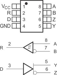
D Package
8-Pin SOIC
Top View

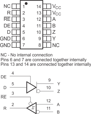
D Package
14-Pin SOIC
Top View

Pin Functions
| PIN | TYPE | DESCRIPTION | ||
|---|---|---|---|---|
| NAME | D (8-PIN) |
D (14-PIN) |
||
| A | 8 | 12 | Bus input | Receiver input (complementary to B) |
| B | 7 | 11 | Bus input | Receiver input (complementary to A) |
| D | 3 | 5 | Digital input | Driver data input |
| DE | — | 4 | Digital input | Driver enable, active high |
| GND | 4 | 6, 7 | Reference potential | Local device ground |
| NC | — | 1, 8 | No connect | No connect; must be left floating |
| R | 2 | 2 | Digital output | Receive data output |
| RE | — | 3 | Digital output | Receiver enable, active low |
| VCC | 1 | 13, 14 | Supply | 3-V to 3.6-V supply |
| Y | 5 | 9 | Bus output | Driver output (complementary to Z) |
| Z | 6 | 10 | Bus output | Driver output (complementary to Y) |