ZHCSRQ0F june 2004 – february 2023 SN65HVD485E
PRODUCTION DATA
- 1 特性
- 2 应用
- 3 说明
- 4 Revision History
- 5 Device Comparison Table
- 6 Pin Configuration and Functions
-
7 Specifications
- 7.1 Absolute Maximum Ratings
- 7.2 ESD Ratings
- 7.3 Recommended Operating Conditions
- 7.4 Thermal Information
- 7.5 Electrical Characteristics: Driver
- 7.6 Electrical Characteristics: Receiver
- 7.7 Power Dissipation Characteristics
- 7.8 Supply Current
- 7.9 Switching Characteristics: Driver
- 7.10 Switching Characteristics: Receiver
- 7.11 Dissipation Ratings
- 7.12 Typical Characteristics
- 8 Detailed Description
- 9 Application and Implementation
- 10Device and Documentation Support
- 11Mechanical, Packaging, and Orderable Information
封装选项
机械数据 (封装 | 引脚)
散热焊盘机械数据 (封装 | 引脚)
订购信息
6 Pin Configuration and Functions
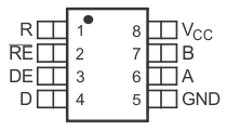
 Figure 6-1 D, DGK, P Packages, 8-Pin SOIC, VSSOP, PDIP
(Top View)
Table 6-1 Pin Functions
| PIN | TYPE | DESCRIPTION | |
|---|---|---|---|
| NAME | NO. | ||
| A | 6 | Bus input/output | Driver output or receiver input (complementary to B) |
| B | 7 | Bus input/output | Driver output or receiver input (complementary to A) |
| D | 4 | Digital input | Driver data input |
| DE | 3 | Digital input | Driver enable, active high |
| GND | 5 | Reference potential | Local device ground |
| R | 1 | Digital input | Receive data output |
| RE | 2 | Digital input | Receiver enable, active low |
| VCC | 8 | Supply | 4.5-V to 5.5-V supply |