ZHCSRQ0F june 2004 – february 2023 SN65HVD485E
PRODUCTION DATA
- 1 特性
- 2 应用
- 3 说明
- 4 Revision History
- 5 Device Comparison Table
- 6 Pin Configuration and Functions
-
7 Specifications
- 7.1 Absolute Maximum Ratings
- 7.2 ESD Ratings
- 7.3 Recommended Operating Conditions
- 7.4 Thermal Information
- 7.5 Electrical Characteristics: Driver
- 7.6 Electrical Characteristics: Receiver
- 7.7 Power Dissipation Characteristics
- 7.8 Supply Current
- 7.9 Switching Characteristics: Driver
- 7.10 Switching Characteristics: Receiver
- 7.11 Dissipation Ratings
- 7.12 Typical Characteristics
- 8 Detailed Description
- 9 Application and Implementation
- 10Device and Documentation Support
- 11Mechanical, Packaging, and Orderable Information
封装选项
机械数据 (封装 | 引脚)
散热焊盘机械数据 (封装 | 引脚)
订购信息
Parameter Measurement Information
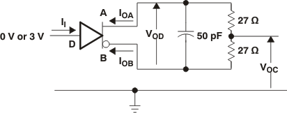 Figure 8-1 Driver Test Circuit, VOD and VOC Without Common-Mode Loading
 Figure 8-2 Driver Test Circuit, VOD With Common-Mode Loading
 Figure 8-3 Driver VOC Test Circuit and Waveforms
 Figure 8-4 Driver Switching Test Circuit and Waveforms
 Figure 8-5 Driver Enable/Disable Test Circuit and Waveforms, High Output
 Figure 8-6 Driver Enable/Disable Test Circuit and Waveforms, Low Output
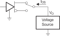 Figure 8-7 Driver Short-Circuit Test
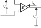 Figure 8-8 Receiver Parameter Definitions
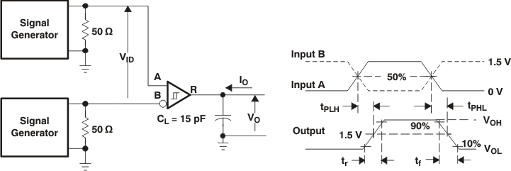 Figure 8-9 Receiver Switching Test Circuit and Waveforms
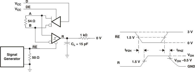 Figure 8-10 Receiver Enable/Disable Test Circuit and Waveforms, Data Output High
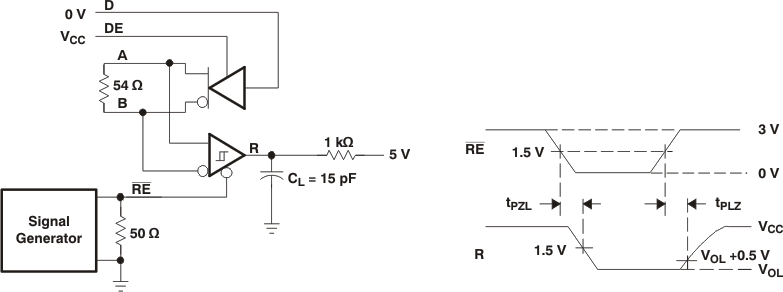 Figure 8-11 Receiver Enable/Disable Test Circuit and Waveforms, Data Output Low
 Figure 8-12 Receiver Enable From Shutdown Test Circuit and Waveforms
 Figure 8-13 Test Circuit and Waveforms, Transient Over-Voltage Test