ZHCSAC4B October 2012 – November 2017 SN65HVD82
PRODUCTION DATA.
9 Application and Implementation
NOTE
Information in the following applications sections is not part of the TI component specification, and TI does not warrant its accuracy or completeness. TI’s customers are responsible for determining suitability of components for their purposes. Customers should validate and test their design implementation to confirm system functionality.
9.1 Application Information
9.1.1 Device Configuration
The SN65HVD82 is a half-duplex, 250-kbps, RS-485 transceiver operating from a single 5-V supply. The driver and receiver enable pins allow for the configuration of different operating modes.
 Figure 15. SN65HVD82 Transceiver Configurations
Using independent enable lines provides the most flexible control as it allows for the driver and the receiver to be turned on and off individually. While this configuration requires two control lines, it allows for selective listening into the bus traffic, whether the driver is transmitting data or not.
Combining the enable signals simplifies the interface to the controller by forming a single, direction-control signal. Thus, when the direction-control line is high, the transceiver is configured as a driver, while for a low the device operates as a receiver.
Tying the receiver-enable to ground and controlling only the driver-enable input, also uses one control line only. In this configuration a node not only receives the data from the bus, but also the data it sends and thus can verify that the correct data have been transmitted.
9.1.2 Bus – Design
An RS-485 bus consists of multiple transceivers connecting in parallel to a bus cable. To eliminate line reflections, each cable end is terminated with a termination resistor, RT, whose value matches the characteristic impedance, Z0, of the cable. This method, known as parallel termination, allows for higher data rates over longer cable length.
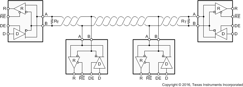 Figure 16. Typical RS-485 Network with SN65HVD82 Transceivers
Common cables used are unshielded twisted pair (UTP), such as low-cost CAT-5 cable with Z0 = 100 Ω, and proper RS-485 cable with Z0 = 120 Ω.
Line measurements have shown that making RT by up to 10% larger than Z0 improves signal quality. Typical cable sizes are AWG 22 and AWG 24.
The theoretical maximum bus length is assumed with 4000 ft or 1200 m, and represents the length of an AWG 24 cable whose cable resistance approaches the value of the termination resistance, thus reducing the bus signal by half or 6 dB.
The theoretical maximum number of bus nodes is determined by the ratio of the RS-485 specified maximum of 32 unit loads (UL) and the actual unit load of the applied transceiver. For example, the SN65HVD82 is a 1/8 UL transceiver. Dividing 32 UL by 1/8 UL yields 256 transceivers that can be connected to one bus.
9.1.3 Cable-Length Versus Data Rate
There is an inverse relationship between data rate and cable length. That is, the higher the data rate the shorter the cable and conversely the lower the data rate the longer the cable. While most RS-485 systems utilize data rates between 10 kbps and 100 kbps, applications such as e-metering often operate at rates of up to 250 kbps even at distances of 4000 feet and above. This is possible by allowing for small signal jitter of up to 5 or 10%.
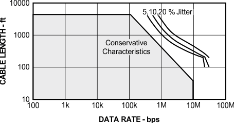 Figure 17. Cable Length vs Data Rate Characteristic
9.1.4 Stub – Length
When connecting a node to the bus, the distance between the transceiver inputs and the cable trunk, known as the stub, should be as short as possible. The reason for this is that a stub presents a non-terminated piece of bus line which can introduce reflections if too long. As a rule of thumb the electrical length or round-trip delay of a stub should be less than one tenth of the driver’s rise time, thus leading to a maximum physical stub length of: LStub ≤ 0.1 × tr × v × c, with tr as the driver’s 10/90 rise time, c as the speed of light (3 × 10⁸ m/s or 9.8 × 108 ft/s), and v as the signal velocity of the cable (v = 78%) or trace (v = 45%) as a factor of c.
Thus, for the SN65HVD82 with a minimum rise time of 400 ns the maximum cable stub length yields LStub ≤ 0.1 × 400 × 10-9 × 3 108 × 0.78 = 9.4 m or 30.6 ft.
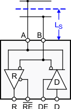 Figure 18. Stub Length
9.1.5 3-V to 5-V Interface
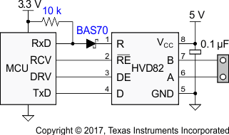
Interfacing the SN65HVD82 to a 3-V controller is easy. Because the 5-V logic inputs of the transceiver accept 3-V input signals they can be directly connected to the controller I/O. The 5-V receiver output, R, however must be level-shifted via a Schottky diode and a 10-kV resistor to connect to the controller input. When R is high, the diode is reverse biased and the controller supply potential lies at the controller input. When R is low, the diode is forward biased and conducts. In this case only the diode forward voltage of 0.2 V lies at the controller input.
9.1.6 Noise Immunity
The input sensitivity of a standard RS-485 transceiver is ±200 mV. When the differential input voltage, VID, is greater than +200 mV, the receiver output turns high, for VID ≤ 200 mV the receiver outputs low. Bus voltages in between these levels can cause the receiver output to go high, or low, or even toggle between logic states. Small bus voltages however occur every time during the bus access hand-off from one driver to the next as the low-impedance termination resistors reduce the bus voltage to zero. To prevent receiver output toggling during bus idling, and thus increasing noise immunity, external bias resistors must be applied to create a bus voltage that is greater than the input sensitivity plus any expected differential noise.
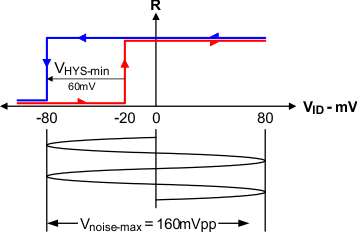 Figure 20. SN65HVD82 Noise Immunity
The SN65HVD82 transceiver circumvents idle-bus and differential noise issues by providing a positive input threshold of –20 mV and a typical hysteresis of 60 mV. In the case of an idle-bus condition therefore, a differential noise voltage of up to 160 mVPP can be present without causing the receiver output to change states from high to low. This increased noise immunity eliminates the need for idle-bus failsafe bias resistors and allows for long haul data transmissions in noisy environment.
9.1.7 Transient Protection
The bus terminals of the SN65HVD82 transceiver family possess on-chip ESD protection against ±15 kV human body model (HBM) and ±12 kV IEC61000-4-2 contact discharge. As stated in the IEC 61000-4-2 standard, contact discharge is the preferred test method; although IEC air-gap testing is less repeatable than contact testing, air discharge protection levels are inferred from the contact discharge test results. The IEC-ESD test is far more severe than the HBM-ESD test. The 50% higher charge capacitance, CS, and 78% lower discharge resistance, RD of the IEC-model produce significantly higher discharge currents than the HBM-model.
 Figure 21. HBM and IEC-ESD Models and Currents in Comparison
EFTs are usually caused by relay contact bounce or the interruption of inductive loads, while surge transients often results from lightning strikes (direct strike or induced voltages and currents due to an indirect strike), or the switching of power systems including load changes and short circuits switching. These transients are often encountered in industrial environments, such as factory automation and power-grid systems.
Figure 22 compares the pulse-power of the EFT and surge transients with the power caused by an IEC-ESD transient. As can be seen the tiny blue blip in the bottom left corner of the left diagram represents the power of a 10-kV ESD transient, which already dwarfs against the significantly higher EFT power spike and certainly against the 500-V surge transient. This type of transient power is well representative for factory environments in industrial and process automation. The right diagram compares the enormous power of a 6-kV surge transient, which more likely occurs in e-metering applications of power generating and power grid systems, with the aforementioned 500-V surge transient. Note that the unit of the pulse-power changes from kW to MW, thus making the power of the 500-V surge transient almost dropping off the scale.
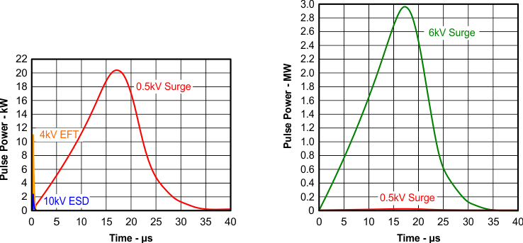 Figure 22. Power Comparison of ESD, EFT, and Surge Transients
In the case of surge transients, their long pulse duration and slowly decreasing pulse power signifies high energy content.
The electrical energy of a transient that is dumped onto the transceiver’s internal protections cells is converted into thermal energy, or heat that literally fries the protection cells, thus destroying the transceiver. Figure 23 showcases the large differences in transient energies for single ESD, EFT, and surge transients as well as for an EFT pulse train, commonly applied during compliance testing.
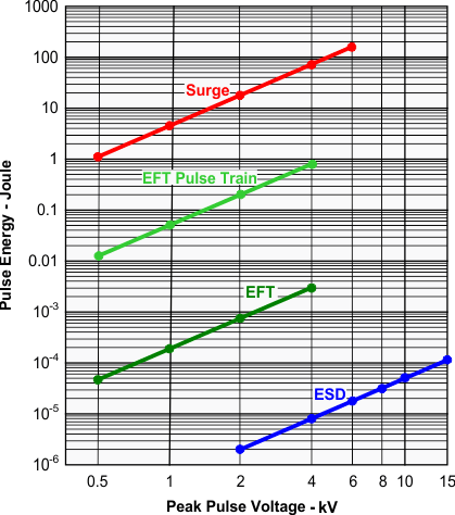 Figure 23. Comparison of Transient Energies
Figure 24 suggests two circuit designs providing protection against surge transients. Table 3 presents the associated bill of material.
Table 3. Bill of Materials
| DEVICE | FUNCTION | ORDER NUMBER | MANUFACTURER |
|---|---|---|---|
| XCVR | 3.3V, 250kbps RS-485 Transceiver | SN65HVD82D | TI |
| R1,R2 | 10Ω, Pulse-Proof Thick-Film Resistor | CRCW0603010RJNEAHP | Vishay |
| TVS | Bidirectional 400W Transient Suppressor | CDSOT23-SM712 | Bourns |
| TBU1,TBU2 | Bidirectional. 200mA Transient Blocking Unit | TBU-CA-065-200-WH | Bourns |
| MOV1,MOV2 | 200V, Metal-Oxide Varistor | MOV-10D201K | Bourns |
 Figure 24. Transient Protection Against ESD, EFT, and Surge Transients
Both circuits are designed for 10-kV ESD and 4-kV EFT transient protection. The left however provides surge protection of ≥ 500-V transients only, while the right protection circuits can withstand 5-kV surge transients.
9.2 Typical Application
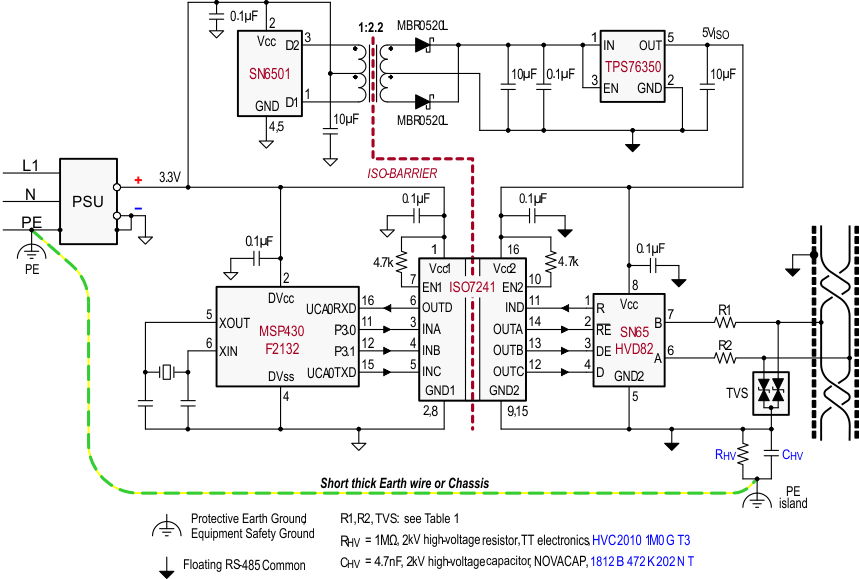 Figure 25. Isolated Bus Node With Transient Protection
9.2.1 Design Requirements
The following list outlines sample design requirements for the typical application example found in Figure 25
- RS-485-compliant bus interface (needs differential signal amplitude of at least 1.5 V under fully-loaded conditions – essentially, maximum number of nodes connected and with dual 120-Ω termination).
- Galvanic isolation of both signal and power supply lines.
- Able to withstand ESD transients up to 10 kV (per IEC 61000-4-2) and EFTs up to 4 kV (per IEC 61000-4-4).
- Full control of data flow on bus in order to prevent contention (for half-duplex communication).
9.2.2 Detailed Design Procedure
9.2.2.1 Custom Design With WEBENCH® Tools
Click here to create a custom design using the SN65HVD82 device with the WEBENCH® Power Designer.
- Start by entering the input voltage (VIN), output voltage (VOUT), and output current (IOUT) requirements.
- Optimize the design for key parameters such as efficiency, footprint, and cost using the optimizer dial.
- Compare the generated design with other possible solutions from Texas Instruments.
The WEBENCH Power Designer provides a customized schematic along with a list of materials with real-time pricing and component availability.
In most cases, these actions are available:
- Run electrical simulations to see important waveforms and circuit performance
- Run thermal simulations to understand board thermal performance
- Export customized schematic and layout into popular CAD formats
- Print PDF reports for the design, and share the design with colleagues
Get more information about WEBENCH tools at www.ti.com/WEBENCH.
9.2.2.2 Isolated Bus Node Design
Many RS-485 networks use isolated bus nodes to prevent the creation of unintended ground loops and their disruptive impact on signal integrity. An isolated bus node typically includes a micro controller that connects to the bus transceiver via a multi-channel, digital isolator (Figure 25).
Power isolation is accomplished using the push-pull transformer driver SN6501 and a low-cost LDO, TPS76350
Signal isolation utilizes the quadruple digital isolator ISO7241. Notice that both enable inputs, EN1 and EN2, are pulled-up via 4.7-kΩ resistors to limit their input currents during transient events.
While the transient protection is similar to the one in Figure 24 (left circuit), an additional high-voltage capacitor is used to divert transient energy from the floating RS-485 common further towards Protective Earth (PE) ground. This is necessary as noise transients on the bus are usually referred to Earth potential.
RVH refers to a high-voltage resistor, and in some applications even a varistor. This resistance is applied to prevent charging of the floating ground to dangerous potentials during normal operation.
Occasionally varistors are used instead of resistors in order to rapidly discharge CHV, if it is expected that fast transients might charge CHV to high-potentials.
Note that the PE island represents a copper island on the PCB for the provision of a short, thick Earth wire connecting this island to PE ground at the entrance of the power supply unit (PSU).
In equipment designs using a chassis, the PE connection is usually provided through the chassis itself. Typically the PE conductor is tied to the chassis at one end while the high-voltage components, CHV and RHV, are connecting to the chassis at the other end.
9.2.3 Application Curve
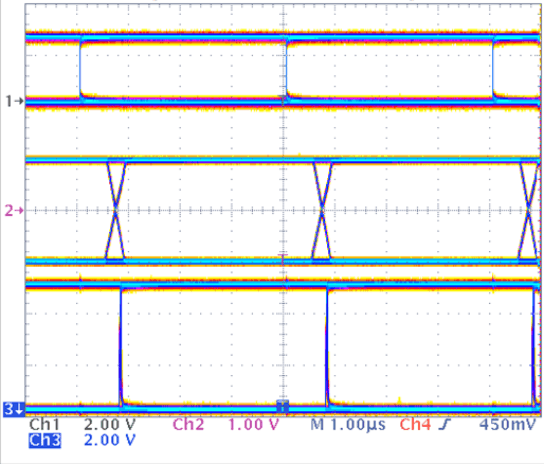 Figure 26. SN65GVD82 D Input (Top), Differential Output (Middle), and R Output (Bottom), 250 kbps Operation, PRBS Data Pattern
