ZHCSB94C July 2013 – January 2018 SN65HVD888
PRODUCTION DATA.
8.3.2 Bus Polarity Correction
The SN65HVD888 automatically corrects a wrong bus-signal polarity caused by a cross-wire fault. In order to detect the bus polarity, all three of the following conditions must be met:
- A failsafe-biasing network (commonly at the master node) must define the signal polarity of the bus
- A slave node must enable the receiver and disable the driver (RE = DE = Low)
- The bus must idle for the failsafe time, tFS-max
After the failsafe time has passed, the polarity correction is complete and is applied to both the receive and transmit channels. The status of the bus polarity is latched within the transceiver and is maintained for subsequent data transmissions.
NOTE
Data string durations of consecutive 0s or 1s exceeding tFS-min can accidently trigger a wrong polarity correction and must be avoided.
Figure 13 shows a simple point-to-point data link between a master node and a slave node. Because the master node with the failsafe biasing network determines the signal polarity on the bus, an RS-485 transceiver without polarity correction, such as SN65HVD82, suffices. All other bus nodes, typically performing as slaves, require the SN65HVD888 transceiver with polarity correction.
 Figure 13. Point-To-Point Data Link With Cross-Wire Fault
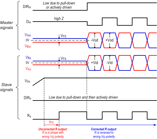
Prior to initiating data transmission the master transceiver must idle for a time span that exceeds the maximum failsafe time, tFS-max, of a slave transceiver. This idle time is accomplished by driving the direction control line, DIR, low. After a time, t > tFS-max, the master begins transmitting data.
Because of the indicated cross-wire fault between master and slave, the slave node receives bus signals with reversed polarity. Assuming the slave node has just been connected to the bus, the direction-control pin is pulled-down during power-up and then is actively driven low by the slave MCU. The polarity correction begins as soon as the slave supply is established and ends after approximately 44 to 76 ms.
 Figure 14. Polarity Correction Timing Prior to a Data Transmission
Initially the slave receiver assumes that the correct bus polarity is applied to the inputs and performs no polarity reversal. Because of the reversed polarity of the bus-failsafe voltage, the output of the slave receiver, RS, turns low. After tFS has passed and the receiver has detected the wrong bus polarity, the internal POLCOR logic reverses the input signal and RS turns high.
At this point all incoming bus data with reversed polarity are polarity corrected within the transceiver. Because polarity correction is also applied to the transmit path, the data sent by the slave MCU are reversed by the POLCOR logic and then fed into the driver.
The reversed data from the slave MCU are reversed again by the cross-wire fault in the bus, and the correct bus polarity is reestablished at the master end.
This process repeats each time the device powers up and detects an incorrect bus polarity.