ZHCSB94C July 2013 – January 2018 SN65HVD888
PRODUCTION DATA.
9.1.7 Transient Protection
The bus terminals of the SN65HVD888 transceiver family possess on-chip ESD protection against ±16 kV HBM and ±12 kV IEC61000-4-2 contact discharge. The International Electrotechnical Commision (IEC) ESD test is far more severe than the HBM ESD test. The 50% higher charge capacitance, CS, and 78% lower discharge resistance, RD of the IEC model produce significantly higher discharge currents than the HBM model.
As stated in the IEC 61000-4-2 standard, contact discharge is the preferred transient protection test method. Although IEC air-gap testing is less repeatable than contact testing, air discharge protection levels are inferred from the contact discharge test results.
 Figure 20. HBM and IEC-ESD Models and Currents in Comparison (HBM Values in Parenthesis)
 The on-chip implementation of IEC ESD protection significantly increases the robustness of equipment. Common discharge events occur because of human contact with connectors and cables. Designers may choose to implement protection against longer duration transients, typically referred to as surge transients. Figure 12 suggests two circuit designs providing protection against short and long duration surge transients, in addition to ESD and Electrical Fast Transients (EFT) transients. Table 4 lists the bill of materials for the external protection devices.
EFTs are generally caused by relay-contact bounce or the interruption of inductive loads. Surge transients often result from lightning strikes (direct strike or an indirect strike which induce voltages and currents), or the switching of power systems, including load changes and short circuits switching. These transients are often encountered in industrial environments, such as factory automation and power-grid systems.
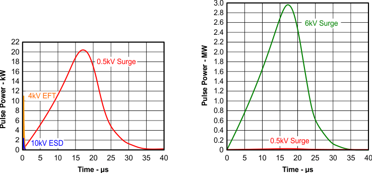
Figure 21 compares the pulse-power of the EFT and surge transients with the power caused by an IEC ESD transient. In the diagram on the left of Figure 21, the tiny blue blip in the bottom left corner represents the power of a 10-kV ESD transient, which already dwarfs against the significantly higher EFT power spike, and certainly dwarfs against the 500-V surge transient. This type of transient power is well representative of factory environments in industrial and process automation. The diagram on the fright of Figure 21 compares the enormous power of a 6-kV surge transient, most likely occurring in e-metering applications of power generating and power grid systems, with the aforementioned 500-V surge transient.
NOTE
The unit of the pulse-power changes from kW to MW, thus making the power of the 500-V surge transient almost dropping off the scale.
 Figure 21. Power Comparison of ESD, EFT, and Surge Transients
In the case of surge transients, hgih-energy content is signified by long pulse duration and slow decaying pulse power
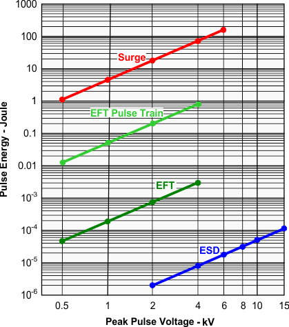
The electrical energy of a transient that is dumped into the internal protection cells of the transceiver is converted into thermal energy. This thermal energy heats the protection cells and literally destroys them, thus destroying the transceiver. Figure 22 shows the large differences in transient energies for single ESD, EFT, and surge transients as well as for an EFT pulse train, commonly applied during compliance testing.
 Figure 22. Comparison of Transient Energies
Table 4. Bill of Materials
| DEVICE | FUNCTION | ORDER NUMBER | MANUFACTURER |
|---|---|---|---|
| XCVR | 5-V, 250-kbps RS-485 Transceiver | SN65HVD888 | TI |
| R1, R2 | 10-Ω, Pulse-Proof Thick-Film Resistor | CRCW0603010RJNEAHP | Vishay |
| TVS | Bidirectional 400-W Transient Suppressor | CDSOT23-SM712 | Bourns |
| TBU1, TBU2 | Bidirectional. | TBU-CA-065-200-WH | Bourns |
| MOV1, MOV2 | 200mA Transient Blocking Unit 200-V, Metal-Oxide Varistor | MOV-10D201K | Bourns |
 Figure 23. Transient Protections Against ESD, EFT, and Surge Transients
The left circuit shown in Figure 23 provides surge protection of ≥ 500-V transients, while the right protection circuits can withstand surge transients of 5 kV.