ZHCSQ22C July 2009 – June 2022 SN65HVDA195-Q1
PRODUCTION DATA
- 1 特性
- 2 应用
- 3 说明
- 4 Revision History
- 5 说明(续)
- 6 Pin Configuration and Functions
- 7 Specifications
- 8 Parameter Measurement Information
-
9 Detailed Description
- 9.1 Overview
- 9.2 Functional Block Diagram
- 9.3 Feature Description
- 9.4 Device Functional Modes
- 10Application and Implementation
- 11Device and Documentation Support
- 12Mechanical, Packaging, and Orderable Information
7.5 Electrical Characteristics
VSUP = 7 V to 27 V, TA = –40°C to 125°C (unless otherwise noted)
| PARAMETER | TEST CONDITIONS | MIN | TYP(1) | MAX | UNIT | |
|---|---|---|---|---|---|---|
| SUPPLY | ||||||
| Operational supply voltage(2) | Device is operational beyond the LIN 2.0 defined nominal supply line voltage range of 7 V ≤ VSUP ≤ 18 V | 7 | 14 | 27 | V | |
| Nominal supply line voltage | Normal and standby modes | 7 | 14 | 18 | ||
| Sleep mode | 7 | 12 | 18 | |||
| VSUP undervoltage threshold | 4.8 | 6 | ||||
| ISUP | Supply current | Normal mode, EN = High, Bus dominant (total bus load where RLIN ≥ 500 Ω and CLIN ≤ 10 nF (see Figure 8-1)(3), INH = VSUP, NWake = VSUP | 1.2 | 7.5 | mA | |
| Standby mode, EN = low, Bus dominant (total bus load where RLIN ≥ 500 Ω and CLIN ≤ 10 nF (see Figure 8-1)(3), INH = VSUP, NWake = VSUP | 1 | 2.1 | ||||
| Normal mode, EN = High, Bus recessive, LIN = VSUP, INH = VSUP, NWake = VSUP | 450 | 775 | μA | |||
| Standby mode, EN = Low, Bus recessive, LIN = VSUP, INH = VSUP, NWake = VSUP | 450 | 775 | ||||
| Sleep mode, EN = 0, TA = –40°C to 95°C, 7 V < VSUP ≤ 12 V, LIN = VSUP, NWake = VSUP | 13 | 26 | ||||
| Sleep mode, EN = 0, TA = –40°C to 95°C, 12 V < VSUP < 18 V, LIN = VSUP, NWake = VSUP | 35 | |||||
| ΔISUP | Delta supply current in sleep mode | Sleep mode, EN = 0, TA = –40°C to 95°C, Supply line voltage range of 7 V ≤ VSUP ≤ 18 V, LIN bus voltage: VSUP – 1.85 V ≤ LIN ≤ VSUP | 20 | |||
| RXD OUTPUT PIN | ||||||
| VO | Output voltage | –0.3 | 5.5 | V | ||
| IOL | Low-level output current, open drain | LIN = 0 V, RXD = 0.4 V | 3.5 | mA | ||
| IIKG | Leakage current, high-level | LIN = VSUP, RXD = 5 V | –5 | 0 | 5 | μA |
| TXD INPUT PIN | ||||||
| VIL | Low-level input voltage | –0.3 | 0.8 | V | ||
| VIH | High-level input voltage | 2 | 5.5 | |||
| VIT | Input threshold hysteresis voltage | 30 | 500 | mV | ||
| Pulldown resistor | 125 | 350 | 800 | kΩ | ||
| IIL | Low-level input current | TXD = Low | –5 | 0 | 5 | μA |
| LIN PIN (REFERENCED TO VSUP) | ||||||
| VOH | High-level output voltage | LIN recessive, TXD = High, IO = 0 mA, VSUP = 14 V | VSUP – 1 | V | ||
| VOL | Low-level output voltage | LIN dominant, TXD = Low, IO = 40 mA, VSUP = 14 V | 0 | 0.2 × VSUP | ||
| Rresponder | Pullup resistor to VSUP | Normal and standby modes | 20 | 30 | 60 | kΩ |
| Pullup current source to VSUP | Sleep mode, VSUP = 14 V, LIN = GND | –2 | –20 | μA | ||
| IL | Limiting current | TXD = 0 V | 45 | 160 | 220 | mA |
| TXD = 0 V, TA = –10°C to 125°C | 200 | |||||
| ILKG | Leakage current | LIN = VSUP | –5 | 0 | 5 | μA |
| ILKG | Leakage current, loss of supply | 7 V < LIN ≤ 12 V, VSUP = GND | 5 | |||
| 12 V < LIN < 18 V, VSUP = GND | 10 | |||||
| VIL | Low-level input voltage | LIN dominant | 0.4 × VSUP | V | ||
| VIH | High-level input voltage | LIN recessive | 0.6 × VSUP | |||
| VIT | Input threshold voltage | 0.4 × VSUP | 0.5 × VSUP | 0.6 × VSUP | ||
| Vhys | Hysteresis voltage | 0.05 × VSUP | 0.175 × VSUP | |||
| VIL | Low-level input voltage for wakeup | 0.4 × VSUP | ||||
| EN PIN | ||||||
| VIL | Low-level input voltage | –0.3 | 0.8 | V | ||
| VIH | High-level input voltage | 2 | 5.5 | |||
| Vhys | Hysteresis voltage | 30 | 500 | mV | ||
| Pulldown resistor | 125 | 350 | 800 | kΩ | ||
| IIL | Low-level input current | EN = Low | –5 | 0 | 5 | μA |
| INH PIN | ||||||
| Vo | DC output voltage | –0.3 | VSUP + 0.3 | V | ||
| Ron | On state resistance | Between VSUP and INH, INH = 2-mA drive, Normal or standby mode | 35 | 85 | Ω | |
| IIKG | Leakage current | Low-power mode, 0 < INH < VSUP | –5 | 0 | 5 | μA |
| NWAKE PIN | ||||||
| VIL | Low-level input voltage | –0.3 | VSUP – 3.3 | V | ||
| VIH | High-level input voltage | VSUP – 1 | VSUP + 0.3 | |||
| Pullup current | NWake = 0 V | –45 | –10 | –2 | μA | |
| IIKG | Leakage current | VSUP = NWake | –5 | 0 | 5 | |
| THERMAL SHUTDOWN | ||||||
| Shutdown junction thermal temperature | 190 | °C | ||||
| AC CHARACTERISTICS | ||||||
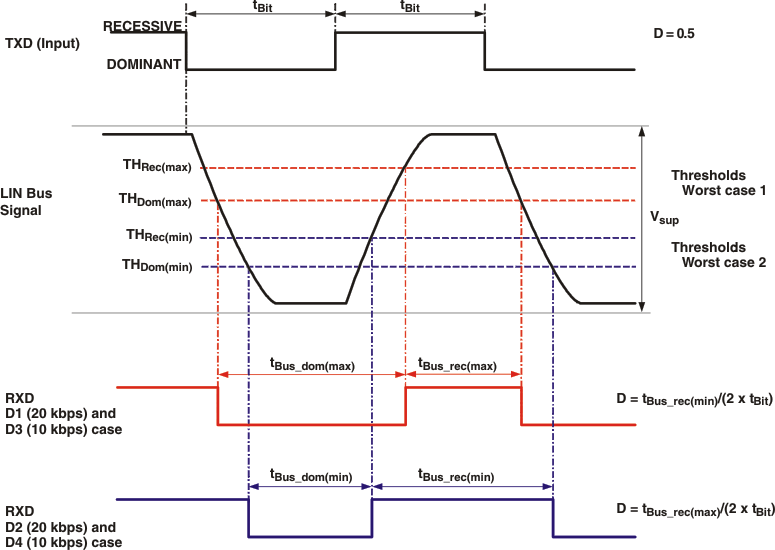
| D1 | Duty cycle 1(4) | THREC(max) = 0.744 × VSUP, THDOM(max) = 0.581 × VSUP, VSUP = 7 V to 18 V, tBIT = 50 μs (20 kbps), D1 = tBus_rec(min)/ (2 × tBIT). See Figure 7-1 | 0.396 | |||
| D2 | Duty cycle 2(4) | THREC(min) = 0.422 × VSUP, THDOM(min) = 0.284 × VSUP, VSUP = 7.6 V to 18 V, tBIT = 50 μs (20 kbps), D2 = tBus_rec(max)/ (2 × tBIT). See Figure 7-1 | 0.581 | |||
| D3 | Duty cycle 3(4) | THREC(max) = 0.778 × VSUP, THDOM(max) = 0.616 × VSUP, VSUP = 7 V to 18 V, tBIT = 96 μs (10.4 kbps), D3 = tBus_rec(min)/ (2 × tBIT). See Figure 7-1 | 0.417 | |||
| D4 | Duty cycle 4(4) | THREC(min) = 0.389 × VSUP, THDOM(min) = 0.251 × VSUP, VSUP = 7.6 V to 18 V, tBIT = 96 μs (10.4 kbps), D4 = tBus_rec(max)/ (2 × tBIT). See Figure 7-1 | 0.59 | |||
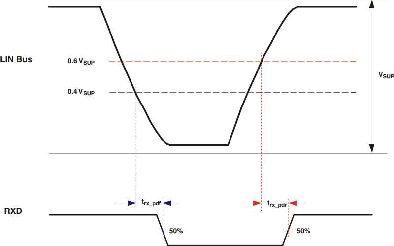
| trx_pdr | Receiver rising propagation delay time | RRXD = 2.4 kΩ, CRXD = 20 pF See Figure 7-2 See Figure 8-1 | 6 | μs | ||
| trx_pdf | Receiver falling propagation delay time | RRXD = 2.4 kΩ, CRXD = 20 pF See Figure 7-2 See Figure 8-1 | 6 | |||
| trx_sym | Symmetry of receiver propagation delay time | rising edge with respect to falling edge (trx_sym = trx_pdf – trx_pdr) RRXD = 2.4 kΩ, CRXD = 20 pF See Figure 7-2 See Figure 8-1 | –2 | 2 | ||
| tNWake | NWake filter time for local wakeup | See Figure 9-4 | 25 | 50 | 150 | |
| tLINBUS | LIN wake-up filter time (dominant time for wakeup through LIN bus) | See Figure 9-3 | 25 | 50 | 150 | |
| tgo_to_operate | See Figure 9-2 to Figure 9-3 | 0.5 | 1 | |||
(1) Typical values are given for VSUP = 14 V at 25°C, except for low power mode where typical values are given for VSUP = 12 V at 25°C.
(2) All voltages are defined with respect to ground; positive currents flow into the SN65HVDA195 device.
(3) In the dominant state, the supply current increases as the supply voltage increases due to the integrated LIN responder termination resistance. At higher voltages the majority of supply current is through the termination resistance. The minimum resistance of the LIN responder termination is 20 kΩ, so the maximum supply current attributed to the termination is:
ISUP (dom) max termination ≉ (VSUP – (VLIN_Dominant + 0.7 V) / 20 kΩ
ISUP (dom) max termination ≉ (VSUP – (VLIN_Dominant + 0.7 V) / 20 kΩ
(4) Duty cycles: LIN driver bus load conditions (CLINBUS, RLINBUS): Load1 = 1 nF, 1 kΩ; Load2 = 10 nF, 500 Ω. Duty cycles 3 and 4 are defined for 10.4-kbps operation. The SN65HVDA195 also meets these lower data rate requirements, while it is capable of the higher speed 20-kbps operation as specified by Duty cycles 1 and 2. SAEJ2602 derives propagation delay equations from the LIN 2.0 duty cycle definitions, for details see the SAEJ2602 specification.
 Figure 7-1 Definition of Bus Timing Parameters
 Figure 7-2 Propagation Delay