SLLS804D March 2009 – August 2016 SN65HVDA540-5-Q1 , SN65HVDA540-Q1 , SN65HVDA541-5-Q1 , SN65HVDA541-Q1 , SN65HVDA542-5-Q1 , SN65HVDA542-Q1
PRODUCTION DATA.
- 1 Features
- 2 Applications
- 3 Description
- 4 Revision History
- 5 Pin Configuration and Functions
- 6 Specifications
- 7 Parameter Measurement Information
- 8 Detailed Description
- 9 Application and Implementation
- 10Power Supply Recommendations
- 11Layout
- 12Device and Documentation Support
- 13Mechanical, Packaging, and Orderable Information
11 Layout
11.1 Layout Guidelines
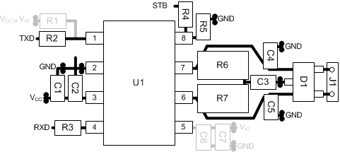
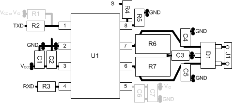
Robust and reliable bus node design often requires the use of external transient protection device to protect against EFT and surge transients that may occur in industrial enviroments. Because ESD and transients have a wide frequency bandwidth from approximately 3 MHz to 3 GHz, high-frequency layout techniques must be applied during PCB design. The HVDA54x-Q1 and HVDA54x-5-Q1 families come with high on-chip IEC ESD protection, but if higher levels of system level immunity are desired external TVS diodes can be used. TVS diodes and bus filtering capacitors should be placed as close to the onboard connectors as possible to prevent noisy transient events from propagating further into the PCB and system.
- Place the protection and filtering circuitry as close to the bus connector, J1, to prevent transients, ESD and noise from propagating onto the board. In this layout example a transient voltage suppression (TVS) device, D1, has been used for added protection. The production solution can be either bidirectional TVS diode or varistor with ratings matching the application requirements. This example also shows optional bus filter capacitors C4 and C5. Additionally (not shown) a series common mode choke (CMC) can be placed on the CANH and CANL lines between the transceiver U1 and connector J1.
- Design the bus protection components in the direction of the signal path. Do not force the transient current to divert from the signal path to reach the protection device.
- Use supply (VCC) and ground planes to provide low inductance.
- Use at least two vias for supply (VCC) and ground connections of bypass capacitors and protection devices to minimize trace and via inductance.
- Bypass and bulk capacitors should be placed as close as possible to the supply terminals of transceiver, examples are C1, C2 on the VCC supply and C6 and C7 on the VIO supply.
- Bus termination: this layout example shows split termination. This is where the termination is split into two resistors, R6 and R7, with the center or split tap of the termination connected to ground via capacitor C3. Split termination provides common mode filtering for the bus. When bus termination is placed on the board instead of directly on the bus, take additional care to ensure the terminating node is not removed from the bus thus also removing the termination. See the application section for information on power ratings needed for the termination resistor(s).
- To limit current of digital lines, serial resistors may be used. Examples are R2, R3, and R4. These are not required.
- Terminal 1: R1 is shown optionally for the TXD input of the device. If an open drain host processor is used, this is mandatory to ensure the bit timing into the device is met.
- Terminal 5: For devices with a VIO input, bypass capacitors should be placed as close to the pin as possible (example C6 and C7). In devices without a VIO input, this pin is not internally connected and can be left floating or tied to any existing net (for example, a split pin connection).
- Terminal 8: is shown assuming the mode terminal, STB, will be used. If the device is only used in normal mode, R4 is not needed and R5 could be used for the pulldown resistor to GND.
NOTE
High-frequency currents follows the path of least impedance and not the path of least resistance.
11.2 Layout Examples
 Figure 28. HVDA540/HVDA541 Layout Example
 Figure 29. HVDA542 Layout Example