ZHCSFI0 September 2016 SN65HVS883
PRODUCTION DATA.
6 Specifications
6.1 Absolute Maximum Ratings
over operating free-air temperature range (unless otherwise noted)| MIN | MAX | UNIT | ||||
|---|---|---|---|---|---|---|
| V24 | Field power input | V24 | –0.3 | 36 | V | |
| VIPx | Field digital inputs | IPx | –0.3 | 36 | V | |
| VID | Voltage at any logic input | DB0, DB1, CLK, SIP, CE, LD | –0.5 | 6 | V | |
| IO | Output current | CHOK, SOP | ±8 | mA | ||
| PTOT | Continuous total power dissipation | See Thermal Information table | ||||
| TJ | Junction temperature | 170 | °C | |||
6.2 ESD Ratings
| VALUE | UNIT | ||||
|---|---|---|---|---|---|
| V(ESD) | Electrostatic discharge | Human-body model (HBM), per ANSI/ESDA/JEDEC JS-001(1) | All pins | ±4000 | V |
| IPx,V24 | ±15000 | ||||
| Charged-device model (CDM), per JEDEC specification JESD22-C101(2) | All pins | ±1000 | |||
| Machine Mode(3) | All pins | ±100 | |||
(1) JEDEC document JEP155 states that 500-V HBM allows safe manufacturing with a standard ESD control process.
(2) JEDEC document JEP157 states that 250-V CDM allows safe manufacturing with a standard ESD control process.
(3) JEDEC Standard 22, Method A115-A.
6.3 Recommended Operating Conditions
| MIN | TYP | MAX | UNIT | ||
|---|---|---|---|---|---|
| V24 | Field supply voltage | 10 | 24 | 34 | V |
| VIPL | Field input low-state input voltage(1) | 0 | 4 | V | |
| VIPH | Field input high-state input voltage(1) | 10 | 34 | V | |
| VIL | Logic low-state input voltage | 0 | 0.8 | V | |
| VIH | Logic high-state input voltage | 2 | 5.5 | V | |
| RLIM | Current limiter resistor | 17 | 25 | 500 | kΩ |
| fIP | Input data rate(2) | 0 | 1 | Mbps | |
| TJ | 150 | °C | |||
| TA | –40 | 85 | °C | ||
(1) Field input voltages correspond to an input resistor of RIN = 1.2 kΩ
(2) Maximum data rate corresponds to 0 ms debounce time, (DB0 = open, DB1 = FGND), and RIN = 0 Ω
6.4 Thermal Information
| THERMAL METRIC(1) | SN65HVS883 | UNIT | ||
|---|---|---|---|---|
| PWP (HTSSOP) | ||||
| 28 PINS | ||||
| RθJA | Junction-to-ambient thermal resistance | 35 | °C/W | |
| RθJC(top) | Junction-to-case (top) thermal resistance | 4.27 | °C/W | |
| RθJB | Junction-to-board thermal resistance | 15 | °C/W | |
| PD | Device power dissipation | ILOAD = 50 mA, RIN = 0, IPO–IP7 = V24 = 30 V, RE7 = FGND, fCLK = 100 MHz, IIP-LIM and ICC = worst case with RLIM = 25 kΩ |
2591 | mW |
(1) For more information about traditional and new thermal metrics, see the Semiconductor and IC Package Thermal Metrics application report.
6.5 Electrical Characteristics
all voltages measured against FGND unless otherwise stated, see Figure 12| SYMBOL | PARAMETER | PIN | TEST CONDITIONS | MIN | TYP | MAX | UNIT |
|---|---|---|---|---|---|---|---|
| VTH–(IP) | Low-level device input threshold voltage | IP0–IP7 | 18 V< V24 < 34 V, RIN = 0 Ω , RLIM = 25 kΩ |
4 | 4.3 | V | |
| VTH+(IP) | High-level device input threshold voltage | 5.2 | 5.5 | V | |||
| VHYS(IP) | Device input hysteresis | 0.9 | V | ||||
| VTH–(IN) | Low-level field input threshold voltage | measured at field side of RIN |
18 V < V24 < 34 V, RIN = 1.2 kΩ ± 5%, RLIM = 25 kΩ |
6 | 8.4 | V | |
| VTH+(IN) | High-level field input threshold voltage | 9.4 | 10 | V | |||
| VHYS(IN) | Field input hysteresis | 1 | V | ||||
| VTH–(V24) | Low-level V24-monitor threshold voltage | V24 | 15 | 16.05 | V | ||
| VTH+(V24) | High-level V24-monitor threshold voltage | 16.8 | 18 | V | |||
| VHYS(V24) | V24-monitor hysteresis | 0.75 | V | ||||
| RIP | Input resistance | IP0–IP7 | 3 V < VIPx < 6 V, RIN = 1.2 kΩ ± 5%, RLIM = 25 kΩ |
1.4 | 1.83 | 2.3 | kΩ |
| IIP-LIM | Input current limit | 10 V < VIPx < 34 V, RLIM = 25 kΩ |
3.15 | 3.6 | 4 | mA | |
| VOL | Logic low-level output voltage | SOP, CHOK | IOL = 20 μA | 0.4 | V | ||
| VOH | Logic high-level output voltage | IOH = –20 μA | 4 | V | |||
| IIL | Logic input leakage current | DB0, DB1, SIP, LD, CE, CLK |
–50 | 50 | μA | ||
| IRE-on | RE on-state current | RE0–RE7 | RLIM = 25 kΩ, REX = FGND |
2.8 | 3.15 | 3.5 | mA |
| ICC(V24) | Supply current | V24 | IP0 to IP7 = V24, 5VOP = open, REX = FGND, All logic inputs open |
8.7 | mA | ||
| VO(5V) | Linear regulator output voltage | 5VOP | 18 V < V24 < 34 V, no load |
4.5 | 5 | 5.5 | V |
| 18 V < V24 < 34 V, IL = 50 mA |
4.5 | 5 | 5.5 | ||||
| ILIM(5V) | Linear regulator output current limit | 115 | mA | ||||
| ΔV5/ΔV24 | Line regulation | 5VOP, V24 | 18 V < V24 < 34 V, IL = 5 mA |
2 | mV/V | ||
| tDB | Debounce times of input channels | IP0–IP7 | DB0 = open, DB1 = FGND |
0 | ms | ||
| DB0 = FGND, DB1 = open |
1 | ||||||
| DB0 = DB1 = open | 3 | ||||||
| tDB-HL | Voltage monitor debounce time after V24 < 15 V (CHOK turns low) | V24, CHOK | 1 | ms | |||
| tDB-LH | Voltage monitor debounce time after V24 > 18 V (CHOK turns high) | 6 | ms | ||||
| TSHDN | Shutdown temperature | 170 | °C |
6.6 Timing Requirements
over operating free-air temperature range (unless otherwise noted)| SYMBOL | PARAMETER | MIN | TYP | MAX | UNIT | |
|---|---|---|---|---|---|---|
| tW1 | CLK pulse width | See Figure 9 | 4 | ns | ||
| tW2 | LD pulse width | See Figure 7 | 6 | ns | ||
| tSU1 | SIP to CLK setup time | See Figure 10 | 4 | ns | ||
| tH1 | SIP to CLK hold time | See Figure 10 | 2 | ns | ||
| tSU2 | Falling edge to rising edge (CE to CLK) setup time | See Figure 11 | 4 | ns | ||
| tREC | LD to CLK recovery time | See Figure 8 | 2 | ns | ||
| fCLK | Clock pulse frequency (50% duty cycle) | See Figure 9 | DC | 100 | MHz | |
6.7 Switching Characteristics
over operating free-air temperature range (unless otherwise noted)| SYMBOL | PARAMETER | TEST CONDITIONS | MIN | TYP | MAX | UNIT |
|---|---|---|---|---|---|---|
| tPLH1, tPHL1 | CLK to SOP | CL = 15 pF, see Figure 9 | 10 | ns | ||
| tPLH2, tPHL2 | LD to SOP | CL = 15 pF, see Figure 7 | 14 | ns | ||
| tr, tf | Rise and fall times | CL = 15 pF, see Figure 9 | 5 | ns |
6.8 Typical Input Characteristics
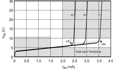
| RIN = 1.2 kΩ | a) IIP-LIM = 2.5 mA (RLIM = 36.1 kΩ) | |||
| b) IIP-LIM = 3.0 mA (RLIM = 30.1 kΩ) | ||||
| c) IIP-LIM = 3.6 mA (RLIM = 24.9 kΩ) | ||||
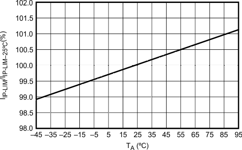
| V24 = 24 V | VIN = 24 V | RIN = 1.2 kΩ |
| RLIM = 24.9 kΩ |
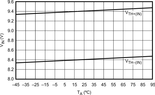
| V24 = 24 V | RIN = 1.2 kΩ | RLIM = 24.9 kΩ |
6.9 Typical Voltage Regulator Performance Characteristics
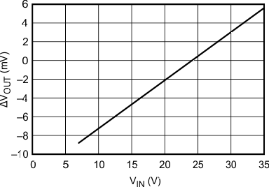
| ILOAD = 5 mA | TA = 27°C | |
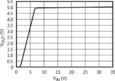
| RLOAD = 100 Ω | ||
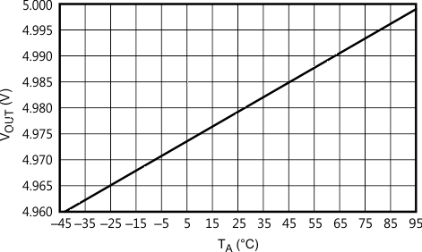
| ILOAD = 0 mA | ||