SLAS638A January   2009  – October 2015 SN65HVS885

PRODUCTION DATA.  

  1. Features
  2. Applications
  3. Description
  4. Revision History
  5. Pin Configuration and Functions
  6. Specifications
    1. 6.1 Absolute Maximum Ratings
    2. 6.2 ESD Ratings
    3. 6.3 Recommended Operating Conditions
    4. 6.4 Thermal Information
    5. 6.5 Electrical Characteristics
    6. 6.6 Timing Requirements
    7. 6.7 Switching Characteristics
    8. 6.8 Typical Characteristics
  7. Parameter Measurement Information
    1. 7.1 Waveforms
    2. 7.2 Signal Conventions
  8. Detailed Description
    1. 8.1 Overview
    2. 8.2 Functional Block Diagram
    3. 8.3 Feature Description
      1. 8.3.1 Digital Inputs
      2. 8.3.2 Debounce Filter
      3. 8.3.3 Shift Register
      4. 8.3.4 Temperature Sensor
    4. 8.4 Device Functional Modes
  9. Application and Implementation
    1. 9.1 Application Information
      1. 9.1.1 System-Level EMC
      2. 9.1.2 Input Channel Switching Characteristics
      3. 9.1.3 Digital Interface Timing
      4. 9.1.4 Cascading for High Channel Count Input Modules
    2. 9.2 Typical Application
      1. 9.2.1 Design Requirements
      2. 9.2.2 Detailed Design Procedure
        1. 9.2.2.1 Input Stage
        2. 9.2.2.2 Setting Debounce Time
        3. 9.2.2.3 Using the HOT Indicator
        4. 9.2.2.4 Example: High-Voltage Sensing Application
      3. 9.2.3 Application Curve
  10. 10Power Supply Recommendations
  11. 11Layout
    1. 11.1 Layout Guidelines
    2. 11.2 Layout Example
  12. 12Device and Documentation Support
    1. 12.1 Community Resources
    2. 12.2 Trademarks
    3. 12.3 Electrostatic Discharge Caution
    4. 12.4 Glossary
  13. 13Mechanical, Packaging, and Orderable Information

封装选项

机械数据 (封装 | 引脚)
散热焊盘机械数据 (封装 | 引脚)
订购信息

5 Pin Configuration and Functions

PWP Package
28-Pin HTSSOP With Exposed Thermal Pad
Top View
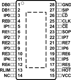
SN65HVS885 po_las638.gif

Pin Functions

PIN DESCRIPTION
NAME NO.
CE 24 Clock Enable Input
CLK 25 Serial Clock Input
DB0 1 Debounce select inputs
DB1 2
GND 28 Device Ground
HOT 16 Over-Temperature Flag
IPx 3, 5, 7, 9,
11, 18, 20, 22
Input Channel x
LD 26 Load Pulse Input
NC 14 Not Connected
REx 4, 6, 8, 10,
12, 17, 19, 21
Return Path x (LED drive)
RLIM 13 Current Limiting Resistor
SIP 27 Serial Data Input
SOP 23 Serial Data Output
VCC 15 5 V Device Supply