ZHCSKH4A October 2006 – November 2019 SN65LBC174A-EP
PRODUCTION DATA.
- 1特性
- 2应用
- 3说明
- 4修订历史记录
- 5说明 (续)
- 6器件和文档支持
- 7机械、封装和可订购信息
封装选项
机械数据 (封装 | 引脚)
散热焊盘机械数据 (封装 | 引脚)
订购信息
5.3 Parameter Measurement Information
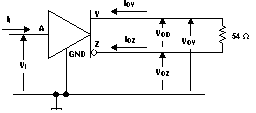 Figure 7. Test Circuit, VOD Without Common-Mode Loading
  Figure 8. Test Circuit, VOD With Common-Mode Loading
PRR = 1 MHz, 50% duty cycle, tr < 6 ns, tf < 6 ns, ZO = 50 Ω
Includes probe and jig capacitance.
Figure 9. VOC Test Circuit 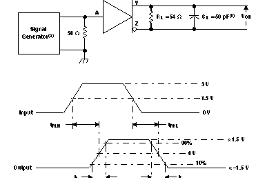
PRR = 1 MHz, 50% duty cycle, tr < 6 ns, tf < 6 ns, ZO = 50 Ω
Includes probe and jig capacitance.
Figure 10. Output Switching Test Circuit and Waveforms 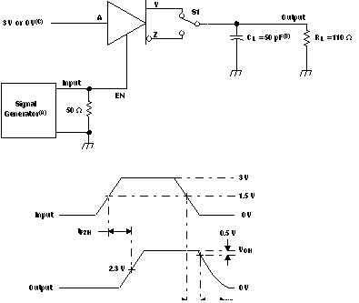
PRR = 1 MHz, 50% duty cycle, tr < 6 ns, tf < 6 ns, ZO = 50 Ω
Includes probe and jig capacitance.
3 V if testing Y output, 0 V if testing Z output.
Figure 11. Enable Timing Test Circuit and Waveforms, TPZH and TPHZ 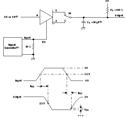
PRR = 1 MHz, 50% duty cycle, tr < 6 ns, tf < 6 ns, ZO = 50 Ω
Includes probe and jig capacitance.
3 V if testing Y output, 0 V if testing Z output.
Figure 12. Enable Timing Test Circuit and Waveforms, TPZL and TPLZ 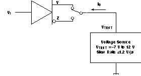 Figure 13. Test Circuit, Short-Circuit Output Current
  Figure 14. Test Circuit Waveform, Transient Overvoltage Test
  Figure 15. Equivalent Input and Output Schematic Diagrams