ZHCSKH4A October   2006  – November 2019 SN65LBC174A-EP

PRODUCTION DATA.  

  1. 1特性
  2. 2应用
  3. 3说明
    1.     Device Images
      1.      逻辑图(正逻辑)
  4. 4修订历史记录
  5. 5说明 (续)
    1. 5.1 Pin Configuration and Functions
      1.      Pin Functions
    2. 5.2 Specifications
      1. 5.2.1 Absolute Maximum Ratings
      2. 5.2.2 ESD Ratings
      3. 5.2.3 Recommended Operating Conditions
      4. 5.2.4 Thermal Information
      5. 5.2.5 Electrical Characteristics
      6. 5.2.6 Switching Characteristics
      7. 5.2.7 Typical Characteristics
    3. 5.3 Parameter Measurement Information
    4. 5.4 Detailed Description
      1. 5.4.1 Overview
      2. 5.4.2 Functional Block Diagram
      3. 5.4.3 Feature Description
      4. 5.4.4 Device Functional Modes
    5. 5.5 Application and Implementation
      1. 5.5.1 Application Information
      2. 5.5.2 Typical Application
        1. 5.5.2.1 Design Requirements
        2. 5.5.2.2 Detailed Design Procedure
        3. 5.5.2.3 Application Curve
    6. 5.6 Power Supply Recommendations
    7. 5.7 Layout
      1. 5.7.1 Layout Guidelines
      2. 5.7.2 Layout Example
  6. 6器件和文档支持
    1. 6.1 接收文档更新通知
    2. 6.2 支持资源
    3. 6.3 商标
    4. 6.4 静电放电警告
    5. 6.5 Glossary
  7. 7机械、封装和可订购信息

封装选项

机械数据 (封装 | 引脚)
散热焊盘机械数据 (封装 | 引脚)
订购信息

Typical Application

The following block diagram shows an MCU host connected via RS-485 to a SPI slave device. This device can be an ADC, DAC, MCU, or other SPI slave peripheral.
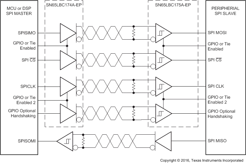
SN65LBC174A-EP fig011_typ_app_cir_sllseu5.gifFigure 16. Typical Application Circuit, MCU Master to Slave Link Via Serial Peripheral Interface