ZHCSFW5 December 2016 SN65LBC175A-EP
PRODUCTION DATA.
8 Detailed Description
8.1 Overview
The SN65LBC175A-EP is a quadruple differential line receiver with tri-state outputs, designed for TIA/EIA-485 (RS-485), TIA/EIA-422 (RS-422), and ISO 8482 (Euro RS-485) applications. This device is optimized for balanced multipoint bus communication at data rates up to and exceeding 50 million bits per second. The transmission media may be twisted-pair cables, printed-circuit board traces, or backplanes. The ultimate rate and distance of data transfer is dependent upon the attenuation characteristics of the media and the noise coupling to the environment.
The receiver operates over a wide range of positive and negative common-mode input voltages, and features ESD protection to 6 kV, making it suitable for high-speed multipoint data transmission applications in harsh environments. These devices are designed using LinBiCMOS®, facilitating low-power consumption and robustness.
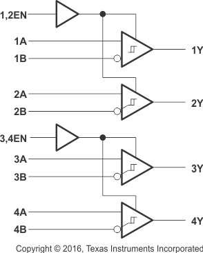
Two EN inputs provide pair-wise enable control, or these can be tied together externally to enable all four drivers with the same signal.
8.2 Functional Block Diagram

8.3 Feature Description
The device can be configured using the enable inputs to select receiver output. The high voltage or logic 1 on the EN pin allows the device to operate on an active-high, and having a low voltage or logic 0 on the EN enables active-low operation. These are simple ways to configure the logic to match the receiving or transmitting controller or microprocessor.
8.4 Device Functional Modes
The receivers implemented in the RS-485 device can be configured using the EN logic pins set to enabled or disabled. This allows users to ignore or filter out transmissions as desired.
Table 1. Function Table(1)
| DIFFERENTIAL INPUTS | ENABLE | OUTPUT | |
|---|---|---|---|
| A - B (VID) | EN | Y | |
| VID ≤ –0.2 V | H | L | |
| –0.2 V < VID < –0.01 V | H | ? | |
| –0.01 V ≤ VID | H | H | |
| X | L | Z | |
| X | OPEN | Z | |
| Short circuit | H | H | |
| Open circuit | H | H | |