ZHCSRD1G May 2000 – February 2023 SN65LBC176A , SN75LBC176A
PRODUCTION DATA
Typical Characteristics
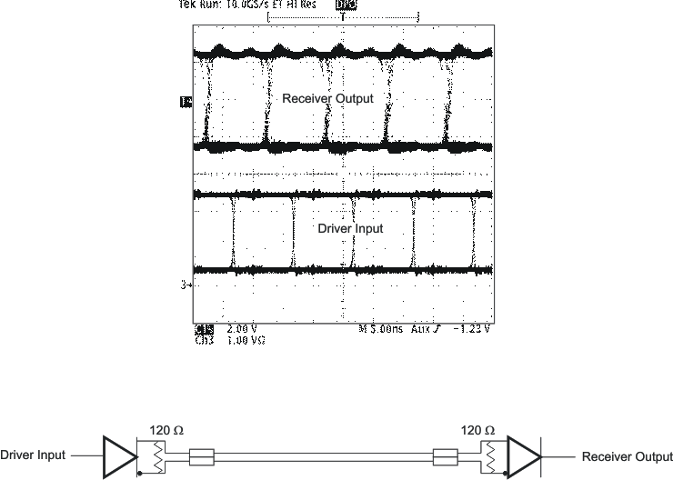 Figure 5-1 Typical Waveform of Non-Return-To-Zero (NRZ), Pseudorandom Binary Sequence (PRBS) Data at 100 Mbps Through 15m, of CAT 5 Unshielded Twisted Pair (UTP) Cable
TIA/EIA-485-A defines a maximum signaling rate as that in which the transition time of the voltage transition of a logic-state change remains less than or equal to 30% of the bit length. Transition times of greater length perform quite well even though they do not meet the standard definition.
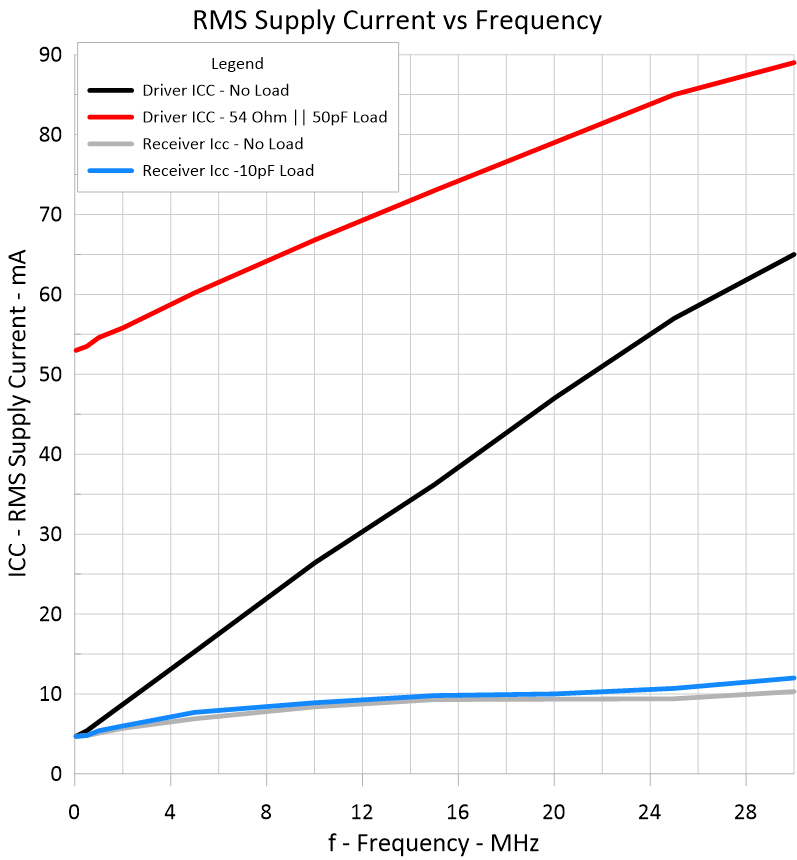 Figure 5-2 RMS Supply Current vs Frequency
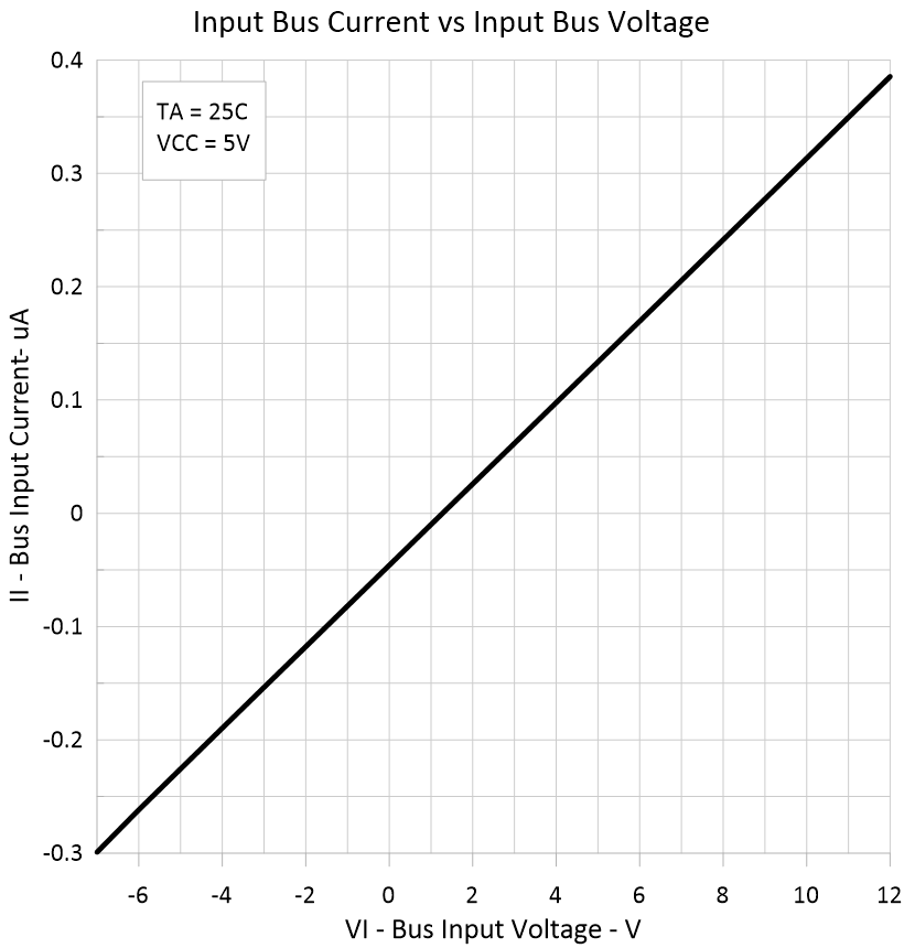 Figure 5-4 Input Current vs Input Voltage
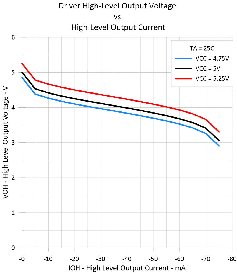 Figure 5-6 Driver High-Level Output Voltage vs High-Level Output Current
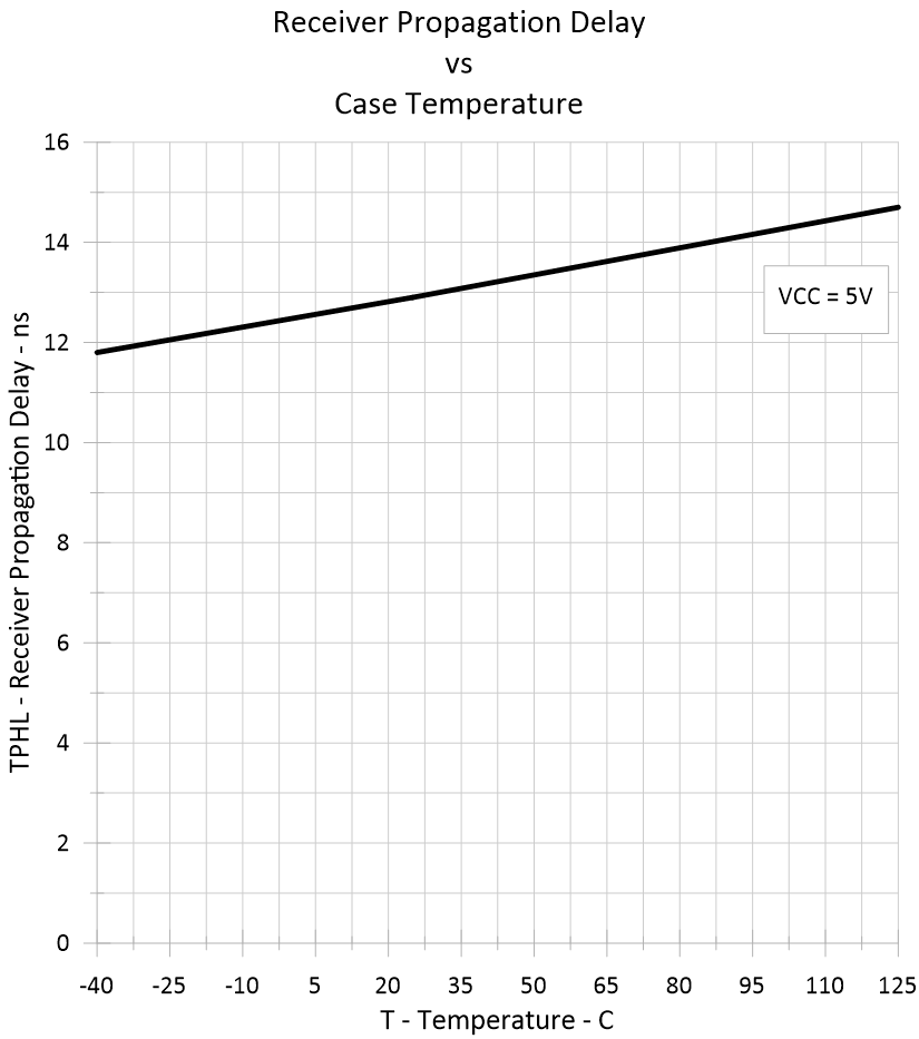 Figure 5-8 Receiver Propagation Time vs Case Temperature
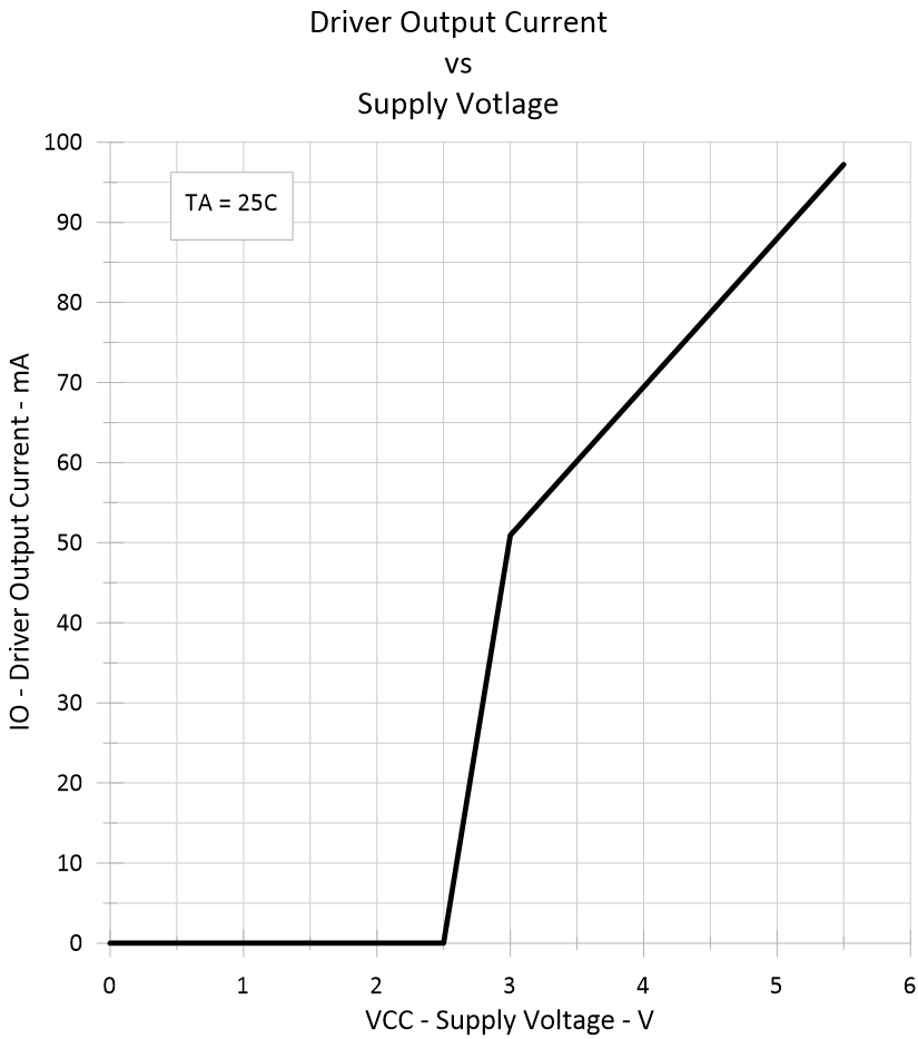 Figure 5-10 Driver Output Current vs Supply Voltage
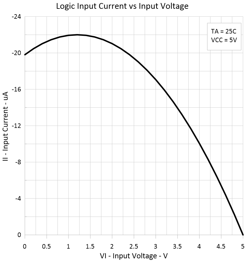 Figure 5-3 Logic Input Current vs Input Voltage
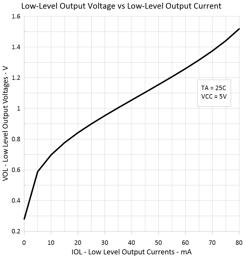 Figure 5-5 Low-Level Output Voltage vs Low-Level Output Current
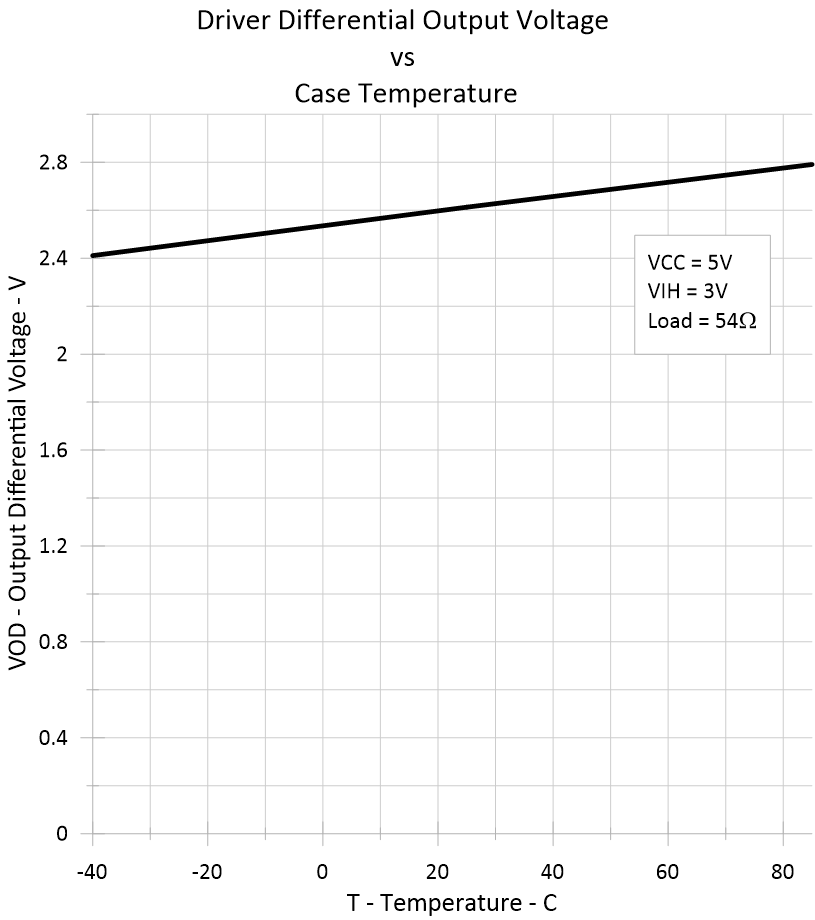 Figure 5-7 Driver Differential Output Voltage vs Case Temperature
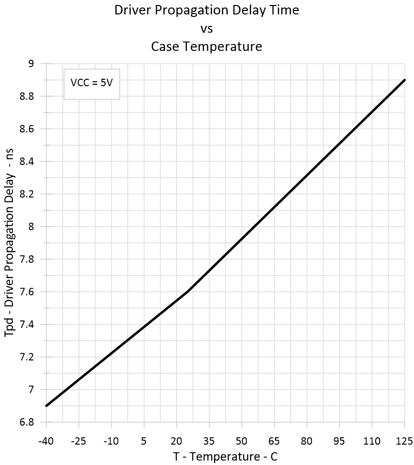 Figure 5-9 Driver Propagation Delay Time vs Case Temperature