ZHCSN67N July 1997 – April 2021 SN55LVDS31 , SN65LVDS31 , SN65LVDS3487 , SN65LVDS9638
PRODUCTION DATA
- 1 特性
- 2 应用
- 3 说明
- 4 Revision History
- 5 说明(续)
- 6 Pin Configuration and Functions
-
7 Specifications
- 7.1 Absolute Maximum Ratings (1)
- 7.2 ESD Ratings
- 7.3 Recommended Operating Conditions
- 7.4 Thermal Information
- 7.5 Electrical Characteristics: SN55LVDS31
- 7.6 Electrical Characteristics: SN65LVDSxxxx
- 7.7 Switching Characteristics: SN55LVDS31
- 7.8 Switching Characteristics: SN65LVDSxxxx
- 7.9 Typical Characteristics
- 8 Parameter Measurement Information
- 9 Detailed Description
- 10Application and Implementation
- 11Power Supply Recommendations
- 12Layout
- 13Device and Documentation Support
- 14Mechanical, Packaging, and Orderable Information
封装选项
请参考 PDF 数据表获取器件具体的封装图。
机械数据 (封装 | 引脚)
- PW|16
- NS|16
- D|16
散热焊盘机械数据 (封装 | 引脚)
订购信息
10.2.1.2.5 PCB Transmission Lines
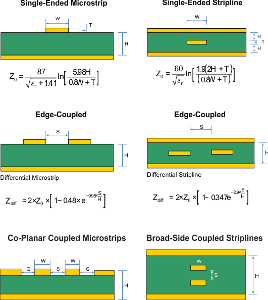
As per SNLA187, #SLLS3731038 depicts several transmission line structures commonly used in printed-circuit boards (PCBs). Each structure consists of a signal line and a return path with uniform cross-section along its length. A microstrip is a signal trace on the top (or bottom) layer, separated by a dielectric layer from its return path in a ground or power plane. A stripline is a signal trace in the inner layer, with a dielectric layer in between a ground plane above and below the signal trace. The dimensions of the structure along with the dielectric material properties determine the characteristic impedance of the transmission line (also called controlled-impedance transmission line).
When two signal lines are placed close by, they form a pair of coupled transmission lines. #SLLS3731038 shows examples of edge-coupled microstrips, and edge-coupled or broad-side-coupled striplines. When excited by differential signals, the coupled transmission line is referred to as a differential pair. The characteristic impedance of each line is called odd-mode impedance. The sum of the odd-mode impedances of each line is the differential impedance of the differential pair. In addition to the trace dimensions and dielectric material properties, the spacing between the two traces determines the mutual coupling and impacts the differential impedance. When the two lines are immediately adjacent; for example, S is less than 2W, the differential pair is called a tightly-coupled differential pair. To maintain constant differential impedance along the length, it is important to keep the trace width and spacing uniform along the length, as well as maintain good symmetry between the two lines.
 Figure 10-4 Controlled-Impedance Transmission Lines