SLLS362G SEPTEMBER 1999 – January 2016 SN65LVDS387 , SN65LVDS389 , SN65LVDS391 , SN75LVDS387 , SN75LVDS389 , SN75LVDS391
PRODUCTION DATA.
- 1 Features
- 2 Applications
- 3 Description
- 4 Revision History
- 5 Description (Continued)
- 6 Device Options
- 7 Pin Configuration and Functions
- 8 Specifications
- 9 Parameter Measurement Information
- 10Detailed Description
- 11Application and Implementation
- 12Power Supply Recommendations
- 13Layout
- 14Device and Documentation Support
- 15Mechanical, Packaging, and Orderable Information
11 Application and Implementation
NOTE
Information in the following applications sections is not part of the TI component specification, and TI does not warrant its accuracy or completeness. TI’s customers are responsible for determining suitability of components for their purposes. Customers should validate and test their design implementation to confirm system functionality.
11.1 Application Information
The intended application of this device and signaling technique is for point-to-point and multidrop baseband data transmission over controlled impedance media of approximately 100 Ω. The transmission media can be printed-circuit board traces, backplanes, or cables. The large number of drivers integrated into the same substrate, along with the low pulse skew of balanced signaling, allows extremely precise timing alignment of clock and data for synchronous parallel data transfers. When used with the companion 16- or 8-channel receivers, the SN65LVDS386 or SN65LVDS388, over 200 million data transfers per second in single-edge clocked systems are possible with very little power.
NOTE
The ultimate rate and distance of data transfer is dependent upon the attenuation characteristics of the media, the noise coupling to the environment, and other system characteristics.
11.1.1 Signaling Rate vs Distance
The ultimate data transfer rate over a given cable or trace length involves many variables. Starting with the capabilities of this LVDS driver to reproduce a data pulse as short as 1.6 ns (a 630-Mbps signaling rate) with less than 500 ps of pulse distortion, any degradation of this pulse by the transmission media will necessarily reduce the timing margin at the receiving end of the data link.
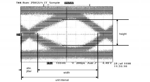
The timing uncertainty induced by the transmission media is commonly referred to as jitter and comes from numerous sources. The characteristics of a particular transmission media can be quantified by using an eye pattern measurement such as shown in Figure 16, which shows about 340 ps of jitter or 20% of the data pulse width.
 Figure 16. Typical LVDS Eye Pattern
A generally accepted range of jitter at the receiver inputs that allows data recovery is 5% to 20% of the unit interval (data pulse width). Table 2 shows the signaling rate achieved on various cables and lengths at a 5% eye pattern jitter with a typical LVDS driver.
Table 2. Signaling Rates for Various Cables for 5% Eye Pattern Jitter
| LENGTH (m) |
CABLE | |||||
|---|---|---|---|---|---|---|
| A(1)
(Mbps) |
B(2)
(Mbps) |
C(3)
(Mbps) |
D(4)
(Mbps) |
E(5)
(Mbps) |
F(6)
(Mbps) |
|
| 1 | 240 | 200 | 240 | 270 | 180 | 230 |
| 5 | 205 | 210 | 230 | 250 | 215 | 230 |
| 10 | 180 | 150 | 195 | 200 | 145 | 180 |
During synchronous parallel transfers, skew between the data and clock lines will also reduce the timing margin. This should be accounted for in the system timing budget. Fortunately, the low output skew of this LVDS driver will generally be a small portion of this budget.
11.2 Typical Application
11.2.1 Point-to-Point Communications
The most basic application for LVDS buffers, as found in this data sheet, is for point-to-point communications of digital data, as shown in Figure 17.
 Figure 17. Point-to-Point Topology
A point-to-point communications channel has a single transmitter (driver) and a single receiver. This communications topology is often referred to as simplex. In Figure 17 the driver receives a single-ended input signal and the receiver outputs a single-ended recovered signal. The LVDS driver converts the single-ended input to a differential signal for transmission over a balanced interconnecting media of 100-Ω characteristic impedance. The conversion from a single-ended signal to an LVDS signal retains the digital data payload while translating to a signal whose features are more appropriate for communication over extended distances or in a noisy environment.
11.2.1.1 Design Requirements
| DESIGN PARAMETERS | EXAMPLE VALUE |
|---|---|
| Driver Supply Voltage (VCCD) | 3.0 to 3.6 V |
| Driver Input Voltage | 0.8 to 3.3 V |
| Driver Signaling Rate | DC to 200 Mbps |
| Interconnect Characteristic Impedance | 100 Ω |
| Termination Resistance | 100 Ω |
| Number of Receiver Nodes | 1 |
| Receiver Supply Voltage (VCCR) | 3.0 to 3.6 V |
| Receiver Input Voltage | 0 to 2.4 V |
| Receiver Signaling Rate | DC to 200 Mbps |
| Ground shift between driver and receiver | ±1 V |
11.2.1.2 Detailed Design Procedure
11.2.1.2.1 Driver Supply Voltage
The SNx5LVDSxx driver is operated from a single supply. The device can support operation with a supply as low as 3 V and as high as 3.6 V. The differential output voltage is nominally 340 mV over the complete output range. The minimum output voltage stays within the specified LVDS limits (247 mV to 454 mV) for the complete 3-V to 3.6-V supply range.
11.2.1.2.2 Driver Bypass Capacitance
Bypass capacitors play a key role in power distribution circuitry. Specifically, they create low-impedance paths between power and ground. At low frequencies, a good digital power supply offers very-low-impedance paths between its terminals. However, as higher frequency currents propagate through power traces, the source is quite often incapable of maintaining a low-impedance path to ground. Bypass capacitors are used to address this shortcoming. Usually, large bypass capacitors (10 μF to 1000 μF) at the board-level do a good job up into the kHz range. Due to their size and length of their leads, they tend to have large inductance values at the switching frequencies of modern digital circuitry. To solve this problem, one should resort to the use of smaller capacitors (nF to μF range) installed locally next to the integrated circuit.
Multilayer ceramic chip or surface-mount capacitors (size 0603 or 0805) minimize lead inductances of bypass capacitors in high-speed environments, because their lead inductance is about 1 nH. For comparison purposes, a typical capacitor with leads has a lead inductance around 5 nH.
The value of the bypass capacitors used locally with LVDS chips can be determined by the following formula according to Johnson(1), equations 8.18 to 8.21. A conservative rise time of 200 ps and a worst-case change in supply current of 1 A covers the whole range of LVDS devices offered by Texas Instruments. In this example, the maximum power supply noise tolerated is 200 mV; however, this figure varies depending on the noise budget available in your design. (1)


The following example lowers lead inductance and covers intermediate frequencies between the board-level capacitor (>10 µF) and the value of capacitance found above (0.001 µF). You should place the smallest value of capacitance as close as possible to the chip.
 Figure 18. Recommended LVDS Bypass Capacitor Layout
11.2.1.2.3 Driver Output Voltage
The SNx5LVDSxx driver output is a 1.2-V common-mode voltage, with a nominal differential output signal of 340 mV. This 340 mV is the absolute value of the differential swing (VOD = |V+– V–|). The peak-to-peak differential voltage is twice this value, or 680 mV.
11.2.1.2.4 Interconnecting Media
The physical communication channel between the driver and the receiver may be any balanced paired metal conductors meeting the requirements of the LVDS standard, the key points which will be included here. This media may be a twisted pair, twinax, flat ribbon cable, or PCB traces.
The nominal characteristic impedance of the interconnect should be between 100 Ω and 120 Ω with variation no more than 10% (90 Ω to 132 Ω).
11.2.1.2.5 PCB Transmission Lines
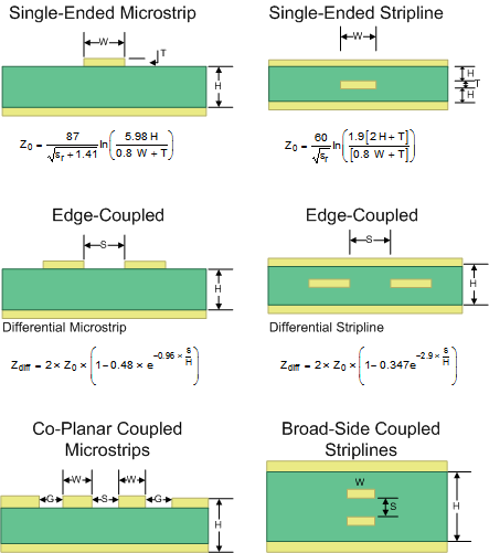
As per SNLA187, Figure 19 depicts several transmission line structures commonly used in printed-circuit boards (PCBs). Each structure consists of a signal line and a return path with uniform cross-section along its length. A microstrip is a signal trace on the top (or bottom) layer, separated by a dielectric layer from its return path in a ground or power plane. A stripline is a signal trace in the inner layer, with a dielectric layer in between a ground plane above and below the signal trace. The dimensions of the structure along with the dielectric material properties determine the characteristic impedance of the transmission line (also called controlled-impedance transmission line).
When two signal lines are placed close by, they form a pair of coupled transmission lines. Figure 19 shows examples of edge-coupled microstrips, and edge-coupled or broad-side-coupled striplines. When excited by differential signals, the coupled transmission line is referred to as a differential pair. The characteristic impedance of each line is called odd-mode impedance. The sum of the odd-mode impedances of each line is the differential impedance of the differential pair. In addition to the trace dimensions and dielectric material properties, the spacing between the two traces determines the mutual coupling and impacts the differential impedance. When the two lines are immediately adjacent; for example, S is less than 2 W, the differential pair is called a tightly-coupled differential pair. To maintain constant differential impedance along the length, it is important to keep the trace width and spacing uniform along the length, as well as maintain good symmetry between the two lines.
 Figure 19. Controlled-Impedance Transmission Lines
11.2.1.2.6 Termination Resistor
As shown earlier, an LVDS communication channel employs a current source driving a transmission line which is terminated with a resistive load. This load serves to convert the transmitted current into a voltage at the receiver input. To ensure incident wave switching (which is necessary to operate the channel at the highest signaling rate), the termination resistance should be matched to the characteristic impedance of the transmission line. The designer should ensure that the termination resistance is within 10% of the nominal media characteristic impedance. If the transmission line is targeted for 100-Ω impedance, the termination resistance should be between 90 Ω and 110 Ω.
The line termination resistance should be located as close as possible to the receiver, thereby minimizing the stub length from the resistor to the receiver. The limiting case would be to incorporate the termination resistor into the receiver, which is exactly what is offered with the TI ‘LVDT receivers.
While we talk in this section about point-to-point communications, a word of caution is useful when a multidrop topology is used. In such topologies, line termination resistors are to be located only at the end(s) of the transmission line. In such an environment, LVDS receivers could be used for loads branching off the main bus with an LVDT receiver used only at the bus end.
11.2.1.2.7 Driver NC Pins
NC (not connected) pins are pins where the die is not physically connected to the lead frame or package. For optimum thermal performance, a good rule of thumb is to ground the NC pins at the board level.
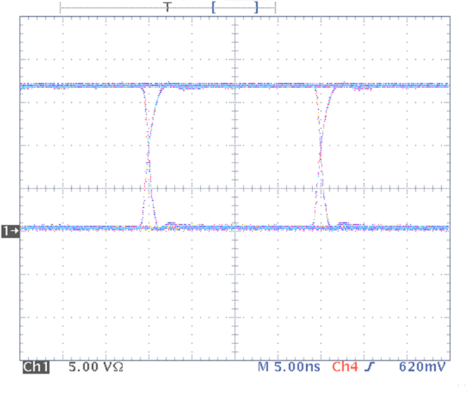
11.2.1.3 Application Curve
 Figure 20. Typical Driver Output Eye Pattern in Point-to-Point System
11.2.2 Multidrop Communications
A second common application of LVDS buffers is a multidrop topology. In a multidrop configuration, a single driver and a shared bus are present along with two or more receivers (with a maximum permissible number of 32 receivers). Figure 21 shows an example of a multidrop system.
 Figure 21. Multidrop Topology
11.2.2.1 Design Requirements
| DESIGN PARAMETERS | EXAMPLE VALUE |
|---|---|
| Driver Supply Voltage (VCCD) | 3.0 to 3.6 V |
| Driver Input Voltage | 0.8 to 3.3 V |
| Driver Signaling Rate | DC to 200 Mbps |
| Interconnect Characteristic Impedance | 100 Ω |
| Termination Resistance | 100 Ω |
| Number of Receiver Nodes | 2 to 32 |
| Receiver Supply Voltage (VCCR) | 3.0 to 3.6 V |
| Receiver Input Voltage | 0 to 2.4 V |
| Receiver Signaling Rate | DC to 200 Mbps |
| Ground shift between driver and receiver | ±1 V |
11.2.2.2 Detailed Design Procedure
11.2.2.2.1 Interconnecting Media
The interconnect in a multidrop system differs considerably from a point-to-point system. While point-to-point interconnects are straightforward and well understood, the bus type architecture encountered with multidrop systems requires more careful attention. We will use Figure 21 above to explore these details.
The most basic multidrop system would include a single driver, located at a bus origin, with multiple receiver nodes branching off the main line, and a final receiver at the end of the transmission line, co-located with a bus termination resistor. While this would be the most basic multidrop system, it has several considerations not yet explored.
The location of the transmitter at one bus end allows the design concerns to be simplified, but this comes at the cost of flexibility. With a transmitter located at the origin, a single bus termination at the far-end is required. The far-end termination absorbs the incident traveling wave. The flexibility lost with this arrangement is thus: if the single transmitter needed to be relocated on the bus, at any location other than the origin, we would be faced with a bus with one open-circuited end, and one properly terminated end. Locating the transmitter say in the middle of the bus may be desired to reduce (by ½) the maximum flight time from the transmitter to receiver.
Another new feature in Figure 21 is clear in that every node branching off the main line results in stubs. The stubs should be minimized in any case, but have the unintended effect of locally changing the loaded impedance of the bus.
To a good approximation, the characteristic transmission line impedance seen into any cut point in the unloaded multipoint or multidrop bus is defined by √L/C, where L is the inductance per unit length and C is the capacitance per unit length. As capacitance is added to the bus in the form of devices and interconnections, the bus characteristic impedance is lowered. This may result in signal reflections from the impedance mismatch between the unloaded and loaded segments of the bus.
If the number of loads is constant and can be distributed evenly along the line, reflections can be reduced by changing the bus termination resistors to match the loaded characteristic impedance. Normally, the number of loads are not constant or distributed evenly and the reflections resulting from any mismatching should be accounted for in the noise budget.
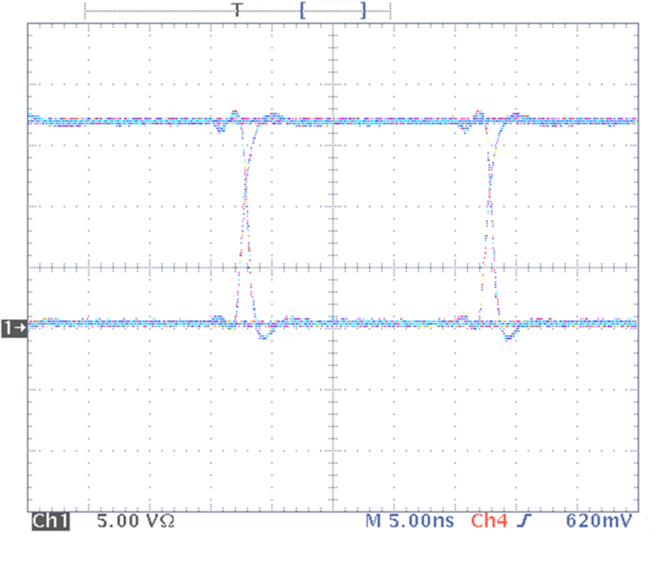
11.2.2.3 Application Curve
 Figure 22. Typical Driver Output Eye Pattern in Multidrop System