SLLS362G SEPTEMBER   1999  – January 2016 SN65LVDS387 , SN65LVDS389 , SN65LVDS391 , SN75LVDS387 , SN75LVDS389 , SN75LVDS391

PRODUCTION DATA.  

  1. Features
  2. Applications
  3. Description
  4. Revision History
  5. Description (Continued)
  6. Device Options
  7. Pin Configuration and Functions
  8. Specifications
    1. 8.1 Absolute Maximum Ratings
    2. 8.2 ESD Ratings
    3. 8.3 Recommended Operating Conditions
    4. 8.4 Thermal Information
    5. 8.5 Electrical Characteristics
    6. 8.6 Switching Characteristics
    7. 8.7 Typical Characteristics
  9. Parameter Measurement Information
  10. 10Detailed Description
    1. 10.1 Overview
    2. 10.2 Functional Block Diagram
    3. 10.3 Feature Description
      1. 10.3.1 Driver Output Voltage and Power-On Reset
      2. 10.3.2 5-V Input Tolerance
      3. 10.3.3 NC Pins
      4. 10.3.4 Unused Enable Pins
      5. 10.3.5 Driver Equivalent Schematics
    4. 10.4 Device Functional Modes
  11. 11Application and Implementation
    1. 11.1 Application Information
      1. 11.1.1 Signaling Rate vs Distance
    2. 11.2 Typical Application
      1. 11.2.1 Point-to-Point Communications
        1. 11.2.1.1 Design Requirements
        2. 11.2.1.2 Detailed Design Procedure
          1. 11.2.1.2.1 Driver Supply Voltage
          2. 11.2.1.2.2 Driver Bypass Capacitance
          3. 11.2.1.2.3 Driver Output Voltage
          4. 11.2.1.2.4 Interconnecting Media
          5. 11.2.1.2.5 PCB Transmission Lines
          6. 11.2.1.2.6 Termination Resistor
          7. 11.2.1.2.7 Driver NC Pins
        3. 11.2.1.3 Application Curve
      2. 11.2.2 Multidrop Communications
        1. 11.2.2.1 Design Requirements
        2. 11.2.2.2 Detailed Design Procedure
          1. 11.2.2.2.1 Interconnecting Media
        3. 11.2.2.3 Application Curve
  12. 12Power Supply Recommendations
  13. 13Layout
    1. 13.1 Layout Guidelines
      1. 13.1.1 Microstrip vs Stripline Topologies
      2. 13.1.2 Dielectric Type and Board Construction
      3. 13.1.3 Recommended Stack Layout
      4. 13.1.4 Separation Between Traces
      5. 13.1.5 Crosstalk and Ground Bounce Minimization
    2. 13.2 Layout Example
  14. 14Device and Documentation Support
    1. 14.1 Device Support
      1. 14.1.1 Third-Party Products Disclaimer
      2. 14.1.2 Other LVDS Products
    2. 14.2 Documentation Support
      1. 14.2.1 Related Information
    3. 14.3 Related Links
    4. 14.4 Trademarks
    5. 14.5 Electrostatic Discharge Caution
    6. 14.6 Glossary
  15. 15Mechanical, Packaging, and Orderable Information

封装选项

请参考 PDF 数据表获取器件具体的封装图。

机械数据 (封装 | 引脚)
  • PW|16
  • D|16
散热焊盘机械数据 (封装 | 引脚)
订购信息

9 Parameter Measurement Information
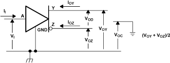
SN65LVDS387 SN75LVDS387 SN65LVDS389 SN75LVDS389 SN65LVDS391 SN75LVDS391 pm_volcurr_lls362.gif Figure 9. Voltage and Current Definitions
SN65LVDS387 SN75LVDS387 SN65LVDS389 SN75LVDS389 SN65LVDS391 SN75LVDS391 pm_vod_lls362.gif Figure 10. VOD Test Circuit
SN65LVDS387 SN75LVDS387 SN65LVDS389 SN75LVDS389 SN65LVDS391 SN75LVDS391 pm_test_cir_lls362.gif

NOTE:

All input pulses are supplied by a generator having the following characteristics: tr or tf ≤ 1 ns, pulse repetition rate (PRR) = 0.5 Mpps, pulse width = 500 ± 10 ns. CL includes instrumentation and fixture capacitance within 0.06 m of the device under test. The measurement of VOC(PP) is made on test equipment with a –3 dB bandwidth of at least 300 MHz.
Figure 11. Test Circuit and Definitions for the Driver Common-Mode Output Voltage
SN65LVDS387 SN75LVDS387 SN65LVDS389 SN75LVDS389 SN65LVDS391 SN75LVDS391 pm_test_cir1_lls362.gif

NOTE:

All input pulses are supplied by a generator having the following characteristics: tr or tf ≤ 1 ns, pulse repetition rate (PRR) = 50 Mpps, pulse width = 10 ± 0.2 ns. CL includes instrumentation and fixture capacitance within 0.06 m of the device under test.
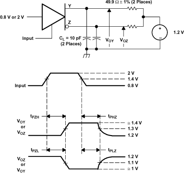
Figure 12. Test Circuit, Timing, and Voltage Definitions for the Differential Output Signal
SN65LVDS387 SN75LVDS387 SN65LVDS389 SN75LVDS389 SN65LVDS391 SN75LVDS391 pm_enable_lls362.gif

NOTE:

All input pulses are supplied by a generator having the following characteristics: tr or tf ≤ 1 ns, pulse repetition rate (PRR) = 0.5 Mpps, pulse width = 500 ± 10 ns. CL includes instrumentation and fixture capacitance within 0.06 m of the device under test.
Figure 13. Enable and Disable Time Circuit and Definitions