ZHCS369A July 2011 – November 2015 SN65LVDS4
PRODUCTION DATA.
- 1 特性
- 2 应用
- 3 说明
- 4 修订历史记录
- 5 Pin Configuration and Functions
-
6 Specifications
- 6.1 Absolute Maximum Ratings
- 6.2 ESD Ratings
- 6.3 Recommended Operating Conditions
- 6.4 Thermal Information
- 6.5 Receiver Electrical Characteristics: VCC = 2.5 V
- 6.6 Receiver Electrical Characteristics: VCC = 1.8 V
- 6.7 Receiver Switching Characteristics: VCC = 2.5 V
- 6.8 Receiver Switching Characteristics: VCC = 1.8 V
- 6.9 Typical Characteristics
- 7 Parameter Measurement Information
- 8 Detailed Description
- 9 Application and Implementation
- 10Power Supply Recommendations
- 11Layout
- 12器件和文档支持
- 13机械、封装和可订购信息
9 Application and Implementation
NOTE
Information in the following applications sections is not part of the TI component specification, and TI does not warrant its accuracy or completeness. TI’s customers are responsible for determining suitability of components for their purposes. Customers should validate and test their design implementation to confirm system functionality.
9.1 Application Information
The SN65LVDS4 device is a single-channel LVDS line receiver. This device is generally useful for building blocks for high-speed, point-to-point, data transmission where ground differences are less than 1 V. LVDS drivers and receivers provide high-speed signaling rates that are often implemented with ECL class devices without the ECL power and dual-supply requirements.
9.2 Typical Application
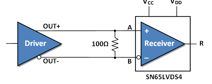
The most basic application for LVDS buffers, as found in this data sheet, is for point-to-point communications of digital data, as shown in Figure 23.
 Figure 23. Point-to-point Topology
A point-to-point communications channel has a single transmitter (driver) and a single receiver. This communications topology is often referred to as simplex. In Figure 23 the driver receives a single-ended input signal and the receiver outputs a single-ended recovered signal. The LVDS driver converts the single-ended input to a differential signal for transmission over a balanced interconnecting media of 100-Ω characteristic impedance. The conversion from a single-ended signal to an LVDS signal retains the digital data payload while translating to a signal whose features are more appropriate for communication over extended distances or in a noisy environment.
9.2.1 Design Requirements
For this design example, use the parameters listed in Table 2.
Table 2. Design Parameters
| DESIGN PARAMETERS | EXAMPLE VALUE |
|---|---|
| Driver Supply Voltage (VCCD) | 3.0 to 3.6 V |
| Driver Input Voltage | 0.8 to 3.3 V |
| Driver Signaling Rate | DC to 500 Mbps |
| Interconnect Characteristic Impedance | 100 Ω |
| Termination Resistance | 100 Ω |
| Number of Receiver Nodes | 1 |
| Receiver Supply Voltage (VCCR) | 1.8 to 2.5 V |
| Receiver Output Drive Voltage (VDDR) | 0 to 3.6 V |
| Receiver Input Voltage | 0 to 24 V |
| Receiver Signaling Rate | DC to 500 Mbps |
| Ground shift between driver and receiver | ±1 V |
9.2.2 Detailed Design Procedure
9.2.2.1 Receiver Bypass Capacitance
Bypass capacitors play a key role in power distribution circuitry. Specifically, they create low-impedance paths between power and ground. At low frequencies, a good digital power supply offers very-low-impedance paths between its terminals. However, as higher frequency currents propagate through power traces, the source is quite often incapable of maintaining a low-impedance path to ground. Bypass capacitors are used to address this shortcoming. Usually, large bypass capacitors (10 µF to 1000 μF) at the board-level do a good job up into the kHz range. Due to their size and length of their leads, they tend to have large inductance values at the switching frequencies of modern digital circuitry. To solve this problem, one should resort to the use of smaller capacitors (nF to μF range) installed locally next to the integrated circuit.
Multilayer ceramic chip or surface-mount capacitors (size 0603 or 0805) minimize lead inductances of bypass capacitors in high-speed environments, because their lead inductance is about 1 nH. For comparison purposes, a typical capacitor with leads has a lead inductance around 5 nH.
The value of the bypass capacitors used locally with LVDS chips can be determined by the following formula according to Johnson(1), equations 8.18 to 8.21. A conservative rise time of 200 ps and a worst-case change in supply current of 1 A covers the whole range of LVDS devices offered by Texas Instruments. In this example, the maximum power supply noise tolerated is 200 mV; however, this figure varies depending on the noise budget available in your design. Howard Johnson & Martin Graham.1993. High Speed Digital Design – A Handbook of Black Magic. Prentice Hall PRT. ISBN number 013395724.


The following example lowers lead inductance and covers intermediate frequencies between the board-level capacitor (>10 µF) and the value of capacitance found above (0.001 µF). You should place the smallest value of capacitance as close as possible to the chip.
 Figure 24. Recommended LVDS Receiver Capacitor Layout
9.2.2.2 Receiver Input Voltage
A standard-compliant LVDS driver output is a 1.2-V common-mode voltage, with a nominal differential output signal of 340 mV. This 340 mV is the absolute value of the differential swing (VOD = |V+ – V–|). The peak-to-peak differential voltage is twice this value, or 680 mV.
9.2.2.3 Interconnecting Media
The physical communication channel between the driver and the receiver may be any balanced paired metal conductors meeting the requirements of the LVDS standard, the key points which will be included here. This media may be a twisted pair, twinax, flat ribbon cable, or PCB traces. The nominal characteristic impedance of the interconnect should be between 100 Ω and 120 Ω with a variation of no more than 10% (90 Ω to 132 Ω).
9.2.2.4 PCB Transmission Lines
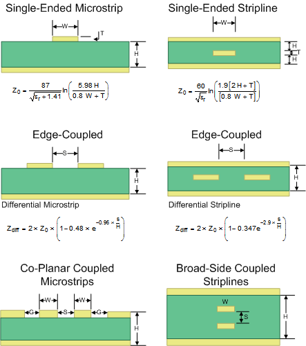
As per SNLA187, Figure 25 depicts several transmission line structures commonly used in printed-circuit boards (PCBs). Each structure consists of a signal line and a return path with uniform cross-section along its length. A microstrip is a signal trace on the top (or bottom) layer, separated by a dielectric layer from its return path in a ground or power plane. A stripline is a signal trace in the inner layer, with a dielectric layer in between a ground plane above and below the signal trace. The dimensions of the structure along with the dielectric material properties determine the characteristic impedance of the transmission line (also called controlled-impedance transmission line).
When two signal lines are placed close by, they form a pair of coupled transmission lines. Figure 25 shows examples of edge-coupled microstrips, and edge-coupled or broad-side-coupled striplines. When excited by differential signals, the coupled transmission line is referred to as a differential pair. The characteristic impedance of each line is called odd-mode impedance. The sum of the odd-mode impedances of each line is the differential impedance of the differential pair. In addition to the trace dimensions and dielectric material properties, the spacing between the two traces determines the mutual coupling and impacts the differential impedance. When the two lines are immediately adjacent; for example, S is less than 2W, the differential pair is called a tightly-coupled differential pair. To maintain constant differential impedance along the length, it is important to keep the trace width and spacing uniform along the length, as well as maintain good symmetry between the two lines.
 Figure 25. Controlled-Impedance Transmission Lines
9.2.2.5 Termination Resistor
An LVDS communication channel employs a current source driving a transmission line which is terminated with a resistive load. This load serves to convert the transmitted current into a voltage at the receiver input. To ensure incident wave switching (which is necessary to operate the channel at the highest signaling rate), the termination resistance should be matched to the characteristic impedance of the transmission line. The designer should ensure that the termination resistance is within 10% of the nominal media characteristic impedance. If the transmission line is targeted for 100-Ω impedance, the termination resistance should be between 90 and 110 Ω.
The line termination resistance should be located as close as possible to the receiver, thereby minimizing the stub length from the resistor to the receiver. The limiting case would be to incorporate the termination resistor into the receiver.
While we talk in this section about point-to-point communications, a word of caution is useful when a multidrop topology is used. In such topologies, line termination resistors are to be located only at the end(s) of the transmission line.
9.2.3 Application Curves
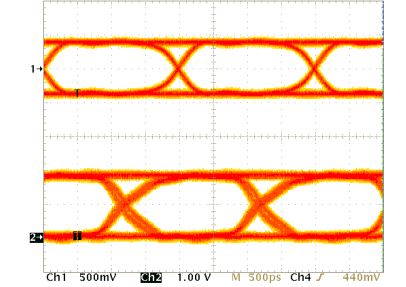
 Figure 26. SN65LVDS4 Operating at 500 Mbps