ZHCS369A July 2011 – November 2015 SN65LVDS4
PRODUCTION DATA.
- 1 特性
- 2 应用
- 3 说明
- 4 修订历史记录
- 5 Pin Configuration and Functions
-
6 Specifications
- 6.1 Absolute Maximum Ratings
- 6.2 ESD Ratings
- 6.3 Recommended Operating Conditions
- 6.4 Thermal Information
- 6.5 Receiver Electrical Characteristics: VCC = 2.5 V
- 6.6 Receiver Electrical Characteristics: VCC = 1.8 V
- 6.7 Receiver Switching Characteristics: VCC = 2.5 V
- 6.8 Receiver Switching Characteristics: VCC = 1.8 V
- 6.9 Typical Characteristics
- 7 Parameter Measurement Information
- 8 Detailed Description
- 9 Application and Implementation
- 10Power Supply Recommendations
- 11Layout
- 12器件和文档支持
- 13机械、封装和可订购信息
8 Detailed Description
8.1 Overview
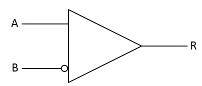
The SN65LVDS4 device is a single-channel LVDS line receiver. It operates from two power supplies, VCC which is the core power supply and VDD which is the output drive power supply. The input signal to the SN65LVDS4 is a differential LVDS signal. The output of the device can be 3.3V LVTTL, 2.5V LVCMOS or 1.8V LVCMOS. This LVDS receiver requires ±50 mV of input signal to determine the correct state of the received signal. The SN65LVDS4 can be used in a point-to-point system or in a multidrop system.
8.2 Functional Block Diagram

8.3 Feature Description
8.3.1 Failsafe
One of the most common problems with differential signaling applications is how the system responds when no differential voltage is present on the signal pair. The LVDS receiver is like most differential line receivers, in that the output logic state can be indeterminate when the differential input voltage is between –50 mV and 50 mV and within its recommended input common-mode voltage range.
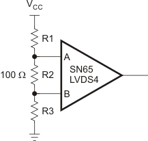
Open circuit means that there is little or no input current to the receiver from the data line itself. This could be when the driver is in a high-impedance state or the cable is disconnected. When this occurs, TI recommends to have an external failsafe solution as shown in Figure 20. In the external failsafe solution, the A side is pulled to VCC via a weak pullup resistor and the B side is pulled down via a weak pulldown resistor. This creates a voltage offset and prevents the receiver from switching based on noise.
 Figure 20. Open-Circuit Failsafe of the LVDS Receiver
8.3.1.1 R1 and R3 Calculation With VCC = 1.8 V
- Assume that an external failsafe bias of 25 mV is desired
- Bias current in this case is = 25 mV/100 Ω = 250 µA
- Next, determine the total resistance from VCC to ground = 1.8 V/250 µA = 7.2 kΩ
- Keeping the common mode bias of 1.25 V to the receiver, the value of R3 = 1.25 V/250 µA = 5 kΩ
- Thus, R1 = 2.2 kΩ
8.3.1.2 R1 and R3 Calculation With VCC = 2.5 V
- Assume that an external failsafe bias of 25 mV is desired
- Bias current in this case is = 25 mV/100 Ω = 250 µA
- Next, determine the total resistance from VCC to ground = 2.5 V/250 µA = 10 kΩ
- Keeping the common mode bias of 1.25 V to the receiver, the value of R3 = 1.25 V/250 µA = 5 kΩ
- Thus, R1 = 5 kΩ
8.4 Device Functional Modes
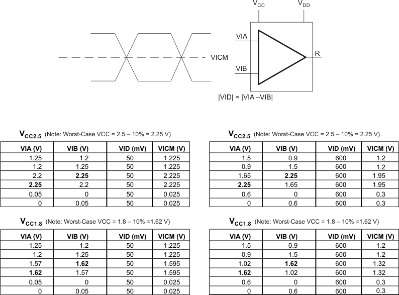
8.4.1 Maximum Input Voltage, VIN(max)
 Figure 21. Maximum Input Voltage Combination Allowed
Table 1. Function Table
| INPUTS | OUTPUT(1) |
|---|---|
| VID = VA – VB | R |
| VID ≥ 50 mV | H |
| VID ≤ –50 mV | L |
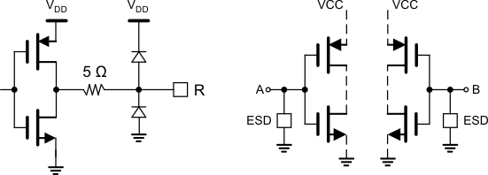
 Figure 22. Receiver Equivalent Input and Output Schematic Diagrams