ZHCSDA2B February 2015 – April 2015 SN65LVDS93A-Q1
PRODUCTION DATA.
6 Specifications
6.1 Absolute Maximum Ratings(1)
| MIN | MAX | UNIT | ||
|---|---|---|---|---|
| Supply voltage range, VCC, IOVCC, LVDSVCC, PLLVCC(2) | –0.5 | 4 | V | |
| Voltage range at any output terminal | –0.5 | VCC + 0.5 | V | |
| Voltage range at any input terminal | –0.5 | IOVCC + 0.5 | V | |
| Continuous power dissipation | See Thermal Information | |||
| Storage temperature, Tstg | –65 | 150 | °C | |
(1) Stresses above these ratings may cause permanent damage. Exposure to absolute maximum conditions for extended periods may degrade device reliability. These are stress ratings only, and functional operation of the device at these or any other conditions beyond those specified is not implied.
(2) All voltages are with respect to the GND terminals.
6.2 ESD Ratings
| VALUE | UNIT | |||
|---|---|---|---|---|
| V(ESD) | Electrostatic discharge | Human-body model (HBM), per AEC Q200-002(1) | ±4000 | V |
| Charged-device model (CDM), per AEC Q100-011 | ±1500 | |||
(1) AEC Q200-002 indicates that HBM stressing shall be in accordance with the ANSI/ESDA/JEDEC JS-001 specification.
6.3 Recommended Operating Conditions
over operating free-air temperature range (unless otherwise noted)| PARAMETER | MIN | NOM | MAX | UNIT | |
|---|---|---|---|---|---|
| Supply voltage, VCC | 3 | 3.3 | 3.6 | V | |
| LVDS output Supply voltage, LVDSVCC | 3 | 3.3 | 3.6 | ||
| PLL analog supply voltage, PLLVCC | 3 | 3.3 | 3.6 | ||
| IO input reference supply voltage, IOVCC | 1.62 | 1.8 / 2.5 / 3.3 | 3.6 | ||
| Power supply noise on any VCC terminal | 0.1 | ||||
| High-level input voltage, VIH | IOVCC = 1.8 V | IOVCC/2 + 0.3 V | V | ||
| IOVCC = 2.5 V | IOVCC/2 + 0.4 V | ||||
| IOVCC = 3.3 V | IOVCC/2 + 0.5 V | ||||
| Low-level input voltage, VIL | IOVCC = 1.8 V | IOVCC/2 - 0.3 V | V | ||
| IOVCC = 2.5 V | IOVCC/2 - 0.4 V | ||||
| IOVCC = 3.3 V | IOVCC/2 - 0.5 V | ||||
| Differential load impedance, ZL | 90 | 132 | Ω | ||
| Operating free-air temperature, TA | –40 | 85 | °C | ||
| Virtual junction temperature, TJ | 105 | °C | |||
6.4 Thermal Information
| THERMAL METRIC(1) | DGG | UNIT | |
|---|---|---|---|
| 56 PINS | |||
| RθJA | Junction-to-ambient thermal resistance | 63.4 | °C/W |
| RθJC(top) | Junction-to-case (top) thermal resistance | 15.9 | |
| RθJB | Junction-to-board thermal resistance | 32.5 | |
| ψJT | Junction-to-top characterization parameter | 0.4 | |
| ψJB | Junction-to-board characterization parameter | 32.2 | |
| RθJC(bot) | Junction-to-case (bottom) thermal resistance | N/A | |
(1) For more information about traditional and new thermal metrics, see the IC Package Thermal Metrics application report, SPRA953.
6.5 Electrical Characteristics
over operating free-air temperature range (unless otherwise noted)| PARAMETER | TEST CONDITIONS | MIN | TYP(1) | MAX | UNIT | |
|---|---|---|---|---|---|---|
| VT | Input voltage threshold | RL = 100Ω, See Figure 7 | IOVCC/2 | V | ||
| |VOD| | Differential steady-state output voltage magnitude | 250 | 450 | mV | ||
| Δ|VOD| | Change in the steady-state differential output voltage magnitude between opposite binary states | 1 | 35 | mV | ||
| VOC(SS) | Steady-state common-mode output voltage | See Figure 7
tR/F (Dx, CLKin) = 1ns |
1.125 | 1.375 | V | |
| VOC(PP) | Peak-to-peak common-mode output voltage | 35 | mV | |||
| IIH | High-level input current | VIH = IOVCC | 25 | μA | ||
| IIL | Low-level input current | VIL = 0 V | ±10 | μA | ||
| IOS | Short-circuit output current | VOY = 0 V | ±24 | mA | ||
| VOD = 0 V | ±12 | mA | ||||
| IOZ | High-impedance state output current | VO = 0 V to VCC | ±20 | μA | ||
| Rpdn | Input pull-down integrated resistor on all inputs (Dx, CLKSEL, SHTDN, CLKIN) | IOVCC = 1.8 V | 200 | kΩ | ||
| IOVCC = 3.3 V | 100 | |||||
| IQ | Quiescent current (average) | disabled, all inputs at GND; SHTDN = VIL |
2 | 100 | μA | |
| ICC | Supply current (average) | SHTDN = VIH, RL = 100Ω (5 places), grayscale pattern (Figure 8) VCC = 3.3 V, fCLK = 75 MHz |
||||
| I(VCC) + I(PLLVCC) + I(LVDSVCC) | 51.9 | mA | ||||
| I(IOVCC) with IOVCC = 3.3 V | 0.4 | |||||
| I(IOVCC) with IOVCC = 1.8 V | 0.1 | |||||
| SHTDN = VIH, RL = 100Ω (5 places), 50% transition density pattern (Figure 8), VCC = 3.3 V, fCLK = 75 MHz |
||||||
| I(VCC) + I(PLLVCC) + I(LVDSVCC) | 53.3 | mA | ||||
| I(IOVCC) with IOVCC = 3.3 V | 0.6 | |||||
| I(IOVCC) with IOVCC = 1.8 V | 0.2 | |||||
| SHTDN = VIH, RL = 100Ω (5 places), worst-case pattern (Figure 9), VCC = 3.6 V, fCLK = 75 MHz |
||||||
| I(VCC) + I(PLLVCC) + I(LVDSVCC) | 63.7 | mA | ||||
| I(IOVCC) with IOVCC = 3.3 V | 1.3 | |||||
| I(IOVCC) with IOVCC = 1.8 V | 0.5 | |||||
| SHTDN = VIH, RL = 100Ω (5 places), worst-case pattern (Figure 9), fCLK = 100 MHz |
||||||
| I(VCC) + I(PLLVCC) + I(LVDSVCC) | 81.6 | mA | ||||
| I(IOVCC) with IOVCC = 3.6 V | 1.6 | |||||
| I(IOVCC) with IOVCC = 1.8 V | 0.6 | |||||
| SHTDN = VIH, RL = 100Ω (5 places), worst-case pattern (Figure 9), fCLK = 135 MHz |
||||||
| I(VCC) + I(PLLVCC) + I(LVDSVCC) | 102.2 | mA | ||||
| I(IOVCC) with IOVCC = 3.6 V | 2.1 | |||||
| I(IOVCC) with IOVCC = 1.8 V | 0.8 | |||||
| CI | Input capacitance | 2 | pF | |||
(1) All typical values are at VCC = 3.3 V, TA = 25°C.
6.6 Timing Requirements
| PARAMETER | MIN | MAX | UNIT | |
|---|---|---|---|---|
| Input clock period, tc | 7.4 | 100 | ns | |
| Input clock modulation | with modulation frequency 30 kHz | 8% | ||
| with modulation frequency 50 kHz | 6% | |||
| High-level input clock pulse width duration, tw | 0.4 tc | 0.6 tc | ns | |
| Input signal transition time, tt | 3 | ns | ||
| Data set up time, D0 through D27 before CLKIN (See Figure 6) | 2 | ns | ||
| Data hold time, D0 through D27 after CLKIN | 0.8 | ns | ||
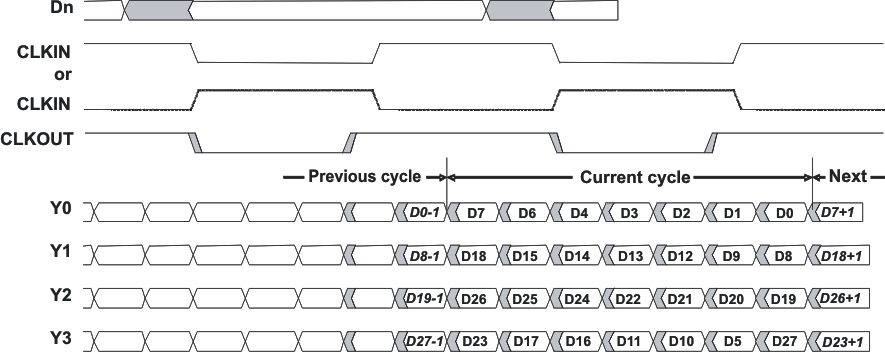 Figure 1. Typical SN65LVDS93A-Q1 Load and Shift Sequences
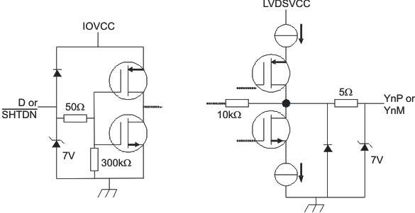 Figure 2. Equivalent Input and Output Schematic Diagrams
6.7 Switching Characteristics
over operating free-air temperature range (unless otherwise noted)| PARAMETER | TEST CONDITIONS | MIN | TYP(1) | MAX | UNIT | |
|---|---|---|---|---|---|---|
| t0 | Delay time, CLKOUT↑ after Yn valid (serial bit position 0, equal D1, D9, D20, D5) | See Figure 10, tC = 10ns, |Input clock jitter| < 25ps (2) |
-0.1 | 0 | 0.1 | ns |
| t1 | Delay time, CLKOUT↑ after Yn valid (serial bit position 1, equal D0, D8, D19, D27) | 1/7 tc - 0.1 | 1/7 tc + 0.1 | ns | ||
| t2 | Delay time, CLKOUT↑ after Yn valid (serial bit position 2, equal D7, D18, D26. D23) | 2/7 tc - 0.1 | 2/7 tc + 0.1 | ns | ||
| t3 | Delay time, CLKOUT↑ after Yn valid (serial bit position 3; equal D6, D15, D25, D17) | 3/7 tc - 0.1 | 3/7 tc + 0.1 | ns | ||
| t4 | Delay time, CLKOUT↑ after Yn valid (serial bit position 4, equal D4, D14, D24, D16) | 4/7 tc - 0.1 | 4/7 tc + 0.1 | ns | ||
| t5 | Delay time, CLKOUT↑ after Yn valid (serial bit position 5, equal D3, D13, D22, D11) | 5/7 tc - 0.1 | 5/7 tc + 0.1 | ns | ||
| t6 | Delay time, CLKOUT↑ after Yn valid (serial bit position 6, equal D2, D12, D21, D10) | 6/7 tc - 0.1 | 6/7 tc + 0.1 | ns | ||
| tc(o) | Output clock period | tc | ns | |||
| Δtc(o) | Output clock cycle-to-cycle jitter (3) | tC = 10ns; clean reference clock, see Figure 11 | ±26 | ps | ||
| tC = 10ns with 0.05UI added noise modulated at 3MHz, see Figure 11 | ±44 | |||||
| tC = 7.4ns; clean reference clock, see Figure 11 | ±35 | |||||
| tC = 7.4ns with 0.05UI added noise modulated at 3MHz, see Figure 11 | ±42 | |||||
| tw | High-level output clock pulse duration | 4/7 tc | ns | |||
| tr/f | Differential output voltage transition time (tr or tf) | See Figure 7 | 225 | 500 | ps | |
| ten | Enable time, SHTDN↑ to phase lock (Yn valid) | f(clk) = 135 MHz, See Figure 12 | 6 | µs | ||
| tdis | Disable time, SHTDN↓ to off-state (CLKOUT high-impedance) | f(clk) = 135 MHz, See Figure 13 | 7 | ns | ||
(1) All typical values are at VCC = 3.3 V, TA = 25°C.
(2) |Input clock jitter| is the magnitude of the change in the input clock period.
(3) The output clock cycle-to-cycle jitter is the largest recorded change in the output clock period from one cycle to the next cycle observed over 15,000 cycles.Tektronix TDSJIT3 Jitter Analysis software was used to derive the maximum and minimum jitter value.
6.8 Typical Characteristics
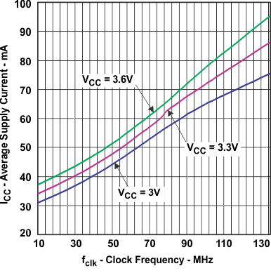
| Total Device Current (Using Grayscale pattern) Over Pixel Clock Frequency |
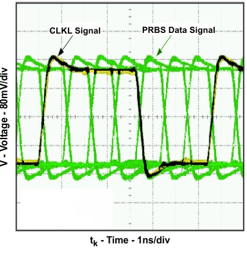
| Clock Signal = 135 MHz | ||
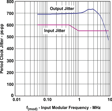
| CLK Frequency During Test = 100 MHz | ||