ZHCSJD7C April 2002 – February 2019 SN65LVDT14 , SN65LVDT41
PRODUCTION DATA.
- 1 特性
- 2 应用
- 3 说明
- 4 修订历史记录
- 5 Pin Configuration and Functions
-
6 Specifications
- 6.1 Absolute Maximum Ratings
- 6.2 ESD Ratings
- 6.3 Recommended Operating Conditions
- 6.4 Thermal Information
- 6.5 Receiver Electrical Characteristics
- 6.6 Driver Electrical Characteristics
- 6.7 Device Electrical Characteristics
- 6.8 Receiver Switching Characteristics
- 6.9 Driver Switching Characteristics
- 6.10 Typical Characteristics
- 7 Parameter Measurement Information
- 8 Detailed Description
- 9 Application and Implementation
- 10Power Supply Recommendations
- 11Layout
- 12器件和文档支持
- 13机械、封装和可订购信息
11.1.3 Recommended Stack Layout
Following the choice of dielectrics and design specifications, the designer must decide how many levels to use in the stack. To reduce the LVCMOS/LVTTL to LVDS crosstalk, it is good practice to have at least two separate signal planes as shown in Figure 25.
 Figure 25. Four-Layer PCB Board
 NOTE
The separation between layers 2 and 3 should be 127 μm (0.005 in). By keeping the power and ground planes tightly coupled, the increased capacitance acts as a bypass for transients.
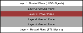
One of the most common stack configurations is the six-layer board, as shown in Figure 26.
 Figure 26. Six-Layer PCB Board
 In this particular configuration, it is possible to isolate each signal layer from the power plane by at least one ground plane. The result is improved signal integrity, but fabrication is more expensive. Using the 6-layer board is preferable, because it offers the layout designer more flexibility in varying the distance between signal layers and referenced planes in addition to ensuring reference to a ground plane for signal layers 1 and 6.