SDLS032H December 1983 – September 2016 SN5407 , SN5417 , SN7407 , SN7417
PRODUCTION DATA.
- 1 Features
- 2 Applications
- 3 Description
- 4 Revision History
- 5 Pin Configuration and Functions
- 6 Specifications
- 7 Parameter Measurement Information
- 8 Detailed Description
- 9 Application and Implementation
- 10Power Supply Recommendations
- 11Layout
- 12Device and Documentation Support
- 13Mechanical, Packaging, and Orderable Information
封装选项
请参考 PDF 数据表获取器件具体的封装图。
机械数据 (封装 | 引脚)
- D|14
- N|14
散热焊盘机械数据 (封装 | 引脚)
订购信息
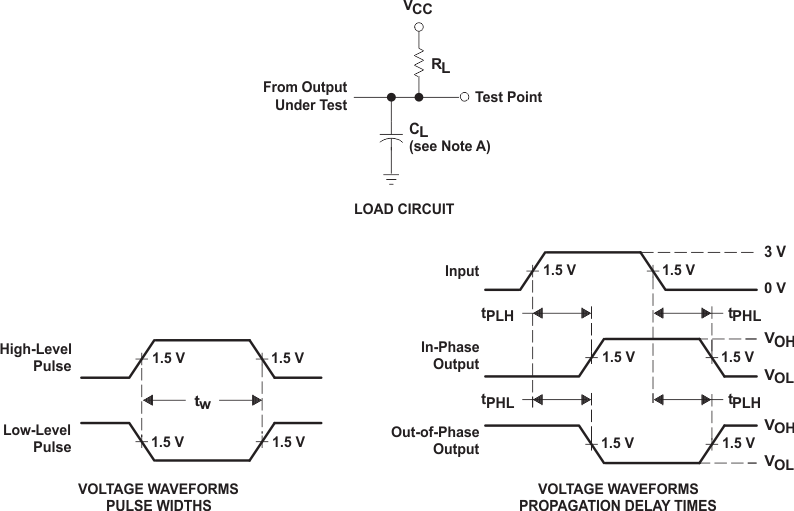
7 Parameter Measurement Information

A. CL includes probe and jig capacitance.
B. In the examples above, the phase relationships between inputs and outputs have been chosen arbitrarily.
C. All input pulses are supplied by generators having the following characteristics: PRR ≤ 1 MHz, ZO = 50 Ω, tr ≤ 7 ns,
tf ≤ 7 ns.
tf ≤ 7 ns.
D. The outputs are measured one at a time, with one input transition per measurement.
Figure 2. Load Circuit and Voltage Waveforms