ZHCSUY0 February   2024 SN74AHC157-Q1

PRODUCTION DATA  

  1.   1
  2. 特性
  3. 应用
  4. 说明
  5. Pin Configuration and Functions
  6. Specifications
    1. 5.1 Absolute Maximum Ratings
    2. 5.2 ESD Ratings
    3. 5.3 Recommended Operating Conditions
    4. 5.4 Thermal Information
    5. 5.5 Electrical Characteristics
    6. 5.6 Switching Characteristics
    7. 5.7 Noise Characteristics
    8. 5.8 Typical Characteristics
  7. Parameter Measurement Information
  8. Detailed Description
    1. 7.1 Overview
    2. 7.2 Functional Block Diagram
    3. 7.3 Feature Description
      1. 7.3.1 Balanced CMOS Push-Pull Outputs
      2. 7.3.2 Standard CMOS Inputs
      3. 7.3.3 Wettable Flanks
      4. 7.3.4 Clamp Diode Structure
    4. 7.4 Device Functional Modes
  9. Application and Implementation
    1. 8.1 Application Information
    2. 8.2 Typical Application
      1. 8.2.1 Design Requirements
        1. 8.2.1.1 Power Considerations
        2. 8.2.1.2 Input Considerations
        3. 8.2.1.3 Output Considerations
      2. 8.2.2 Detailed Design Procedure
      3. 8.2.3 Application Curve
    3. 8.3 Power Supply Recommendations
    4. 8.4 Layout
      1. 8.4.1 Layout Guidelines
      2. 8.4.2 Layout Example
  10. Device and Documentation Support
    1. 9.1 接收文档更新通知
    2. 9.2 支持资源
    3. 9.3 Trademarks
    4. 9.4 静电放电警告
    5. 9.5 术语表
  11. 10Revision History
  12. 11Mechanical, Packaging, and Orderable Information

封装选项

机械数据 (封装 | 引脚)
散热焊盘机械数据 (封装 | 引脚)
订购信息

Clamp Diode Structure

As Figure 7-3 shows, the outputs to this device have both positive and negative clamping diodes, and the inputs to this device have negative clamping diodes only.

CAUTION: Voltages beyond the values specified in the Absolute Maximum Ratings table can cause damage to the device. The input and output voltage ratings may be exceeded if the input and output clamp-current ratings are observed.
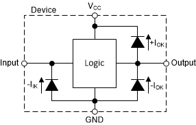
GUID-20200730-CA0I-J186-PPH4-LNSNT76GNZGW-low.gif Figure 7-3 Electrical Placement of Clamping Diodes for Each Input and Output