SCLS264R December 1995 – February 2024 SN54AHCT125 , SN74AHCT125
PRODUCTION DATA
- 1
- 1 Features
- 2 Applications
- 3 Description
- 4 Pin Configuration and Functions
- 5 Specifications
- 6 Parameter Measurement Information
- 7 Detailed Description
- 8 Application and Implementation
- 9 Device and Documentation Support
- 10Revision History
- 11Mechanical, Packaging, and Orderable Information
封装选项
请参考 PDF 数据表获取器件具体的封装图。
机械数据 (封装 | 引脚)
- D|14
- RGY|14
- DB|14
- DGV|14
- PW|14
- BQA|14
- N|14
- NS|14
散热焊盘机械数据 (封装 | 引脚)
- BQA|14
订购信息
3 Description
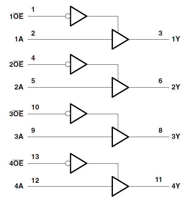
The ’AHCT125 devices are quadruple bus buffer gates featuring independent line drivers with 3-state outputs. Each output is disabled when the associated output-enable (OE) input is high. When OE is low, the respective gate passes the data from the A input to its Y output.
For the high-impedance state during power up or power down, OE should be tied to VCC through a pullup resistor; the minimum value of the resistor is determined by the current-sinking capability of the driver.
Device Information
| PART NUMBER | RATING | PACKAGE(1) |
|---|---|---|
| SN54AHCT125 | Military | J (CDIP, 14) |
| W (CFP, 14) | ||
| FK (LCCC, 20) | ||
| SN74AHCT125 | Commercial | D (SOIC, 14) |
| DB (SSOP, 14) | ||
| DGV (TVSOP, 14) | ||
| N (PDIP, 14) | ||
| NS (SOP, 14) | ||
| PW (SOP, 14) | ||
| RGY (VQFN, 14) | ||
| BQA (WQFN, 14) |
(1) For more information, see Section 11.

Pin numbers are for D, DB, DGV,
J, N, NS, PW, RGY, and W packages.
Logic Diagram (Positive Logic)