ZHCSTE2S March 1996 – February 2024 SN74AHCT1G08
PRODUCTION DATA
- 1
- 1 特性
- 2 应用
- 3 说明
- 4 Pin Configuration and Functions
- 5 Specifications
- 6 Parameter Measurement Information
- 7 Detailed Description
- 8 Application and Implementation
- 9 Device and Documentation Support
- 10Revision History
- 11Mechanical, Packaging, and Orderable Information
封装选项
请参考 PDF 数据表获取器件具体的封装图。
机械数据 (封装 | 引脚)
- DBV|5
- DCK|5
- DRL|5
散热焊盘机械数据 (封装 | 引脚)
订购信息
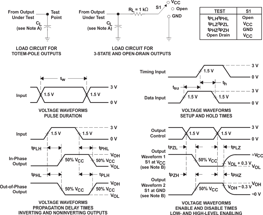
6 Parameter Measurement Information

CL
includes probe and jig capacitance.
Waveform 1 is for
an output with internal conditions such that the output is low except when
disabled by the output control.
Waveform 2 is for an output with internal conditions such that the output is high except when disabled by the output control.
Waveform 2 is for an output with internal conditions such that the output is high except when disabled by the output control.
All input pulses
are supplied by generators having the following characteristics: PRR ≤ 1 MHz,
ZO = 50 Ω, tr ≤ 3 ns, tf ≤ 3 ns.
The outputs are
measured one at a time with one input transition per measurement.
All parameters
and waveforms are not applicable to all devices.
Figure 6-1 Load
Circuit and Voltage Waveforms