ZHCSR74F March   2005  – October 2024 SN74AHCT1G32-Q1

PRODUCTION DATA  

  1.   1
  2. 特性
  3. 应用
  4. 说明
  5. Pin Configuration and Functions
  6. Specifications
    1. 5.1 Absolute Maximum Ratings
    2. 5.2 ESD Ratings
    3. 5.3 Recommended Operating Conditions
    4. 5.4 Thermal Information
    5. 5.5 Electrical Characteristics
    6. 5.6 Switching Characteristics
    7. 5.7 Operating Characteristics
  7. Parameter Measurement Information
  8. Detailed Description
    1. 7.1 Overview
    2. 7.2 Functional Block Diagram
    3. 7.3 Feature Description
    4. 7.4 Device Functional Modes
  9. Application and Implementation
    1. 8.1 Typical Application
      1. 8.1.1 Design Requirements
        1. 8.1.1.1 Power Considerations
        2. 8.1.1.2 Input Considerations
        3. 8.1.1.3 Output Considerations
      2. 8.1.2 Detailed Design Procedure
      3. 8.1.3 Application Curves
    2. 8.2 Power Supply Recommendations
    3. 8.3 Layout
      1. 8.3.1 Layout Guidelines
        1. 8.3.1.1 Layout Example
  10. Device and Documentation Support
    1. 9.1 Documentation Support (Analog)
      1. 9.1.1 Related Documentation
    2. 9.2 接收文档更新通知
    3. 9.3 支持资源
    4. 9.4 Trademarks
    5. 9.5 静电放电警告
    6. 9.6 术语表
  11. 10Revision History
  12. 11Mechanical, Packaging, and Orderable Information

封装选项

机械数据 (封装 | 引脚)
散热焊盘机械数据 (封装 | 引脚)
订购信息

Pin Configuration and Functions

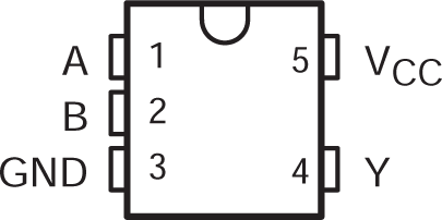
SN74AHCT1G32-Q1 DBV or DCK Package, 5-Pin
                        SOT-23 or SOT-SC70 (Top View)Figure 4-1 DBV or DCK Package, 5-Pin SOT-23 or SOT-SC70 (Top View)
SN74AHCT1G32-Q1 DTX Package, 5-Pin X2SON
                        (Top View)Figure 4-2 DTX Package, 5-Pin X2SON (Top View)
Table 4-1 Pin Functions
PIN TYPE1 DESCRIPTION
NAME NO.
A 1 I Input A
B 2 I Input B
GND 3 Ground Pin
Y 4 O Output Y
VCC 5 Power Pin
  1. I = Input, O = Output, I/O = Input or Output, G = Ground, P = Power.