ZHCSVW7Q October 1995 – July 2024 SN54AHCT573 , SN74AHCT573
PRODUCTION DATA
- 1
- 1 特性
- 2 应用
- 3 说明
- 4 Pin Configuration and Functions
-
5 Specifications
- 5.1 Absolute Maximum Ratings
- 5.2 ESD Ratings
- 5.3 Recommended Operating Conditions
- 5.4 Thermal Information
- 5.5 Electrical Characteristics
- 5.6 Timing Requirements
- 5.7 Switching Characteristics, SNx4AHCT573
- 5.8 Switching Characteristics, SN54AHCT573
- 5.9 Operating Characteristics
- 5.10 Typical Characteristics
- 6 Parameter Measurement Information
- 7 Detailed Description
- 8 Application and Implementation
- 9 Device and Documentation Support
- 10Revision History
- 11Mechanical, Packaging, and Orderable Information
封装选项
请参考 PDF 数据表获取器件具体的封装图。
机械数据 (封装 | 引脚)
- DGV|20
- DB|20
- N|20
- DW|20
- PW|20
散热焊盘机械数据 (封装 | 引脚)
订购信息
6 Parameter Measurement Information
Phase relationships between waveforms were chosen arbitrarily. All input pulses are supplied by generators having the following characteristics: PRR ≤ 1MHz, ZO = 50Ω, RL = 1kΩ, tt < 3ns, Vt = 1.5V.
For clock inputs, fmax is measured when the input duty cycle is 50%.
The outputs are measured one at a time with one input transition per measurement.

(1) CL includes probe
and test-fixture capacitance.
Figure 6-1 Load Circuit for 3-State
Outputs Figure 6-2 Voltage Waveforms, Pulse
Duration
(1) The greater between
tPLH and tPHL is the same as
tpd.
Figure 6-4 Voltage Waveforms,
Propagation Delays
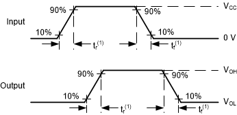
(1) The greater between
tr and tf is the same as tt.
Figure 6-6 Voltage Waveforms, Input
and Output Transition Times Figure 6-3 Voltage Waveforms, Setup
and Hold Times
(1) tPLZ and
tPHZ are the same as tdis.
(2) tPZL and
tPZH are the same as ten.
Figure 6-5 Voltage Waveforms,
Propagation Delays for 3-State Outputs