ZHCSQX3M March 2002 – August 2022 SN74AUC1G125
PRODUCTION DATA
- 1 特性
- 2 应用
- 3 说明
- 4 Revision History
- 5 Pin Configuration and Functions
- 6 Specifications
- 7 Parameter Measurement Information
- 8 Detailed Description
- 9 Application and Implementation
- 10Power Supply Recommendations
- 11Layout
- 12Device and Documentation Support
- 13Mechanical, Packaging, and Orderable Information
封装选项
机械数据 (封装 | 引脚)
散热焊盘机械数据 (封装 | 引脚)
订购信息
5 Pin Configuration and Functions
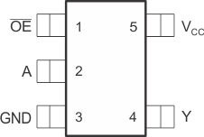
 Figure 5-1 DBV Package,5-Pin SOT-23(Top View)
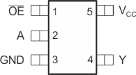
 Figure 5-2 DCK Package,5-Pin SC70(Top View)
Table 5-1 Pin Functions
| PIN | TYPE(1) | DESCRIPTION | ||
|---|---|---|---|---|
| NAME | DBV, DCK | |||
| A | 2 | I | Logic input | |
| GND | 3 | G | Ground | |
| OE | 1 | I | Active-low output enable | |
| VCC | 5 | P | Positive supply | |
| Y | 4 | O | Output | |
(1) I = input, O = output, P = power, G = ground
Figure 5-3 YZP Package,5-Pin DSBGA(Bottom View)
| Legend | |
|---|---|
| Input | Power |
| Ground | Output |
Table 5-2 Pin Functions
| PIN | TYPE(1) | DESCRIPTION | ||
|---|---|---|---|---|
| NO. | NAME | |||
| A1 | OE | I | Output enable, active low | |
| A2 | VCC | P | Positive supply | |
| B1 | A | I | Logic input | |
| C1 | GND | G | Ground | |
| C2 | Y | O | Output | |
(1) I = input, O = output, P = power, G = ground